NO2 Sensing Characteristics of Si MOSFET Gas Sensor Based on Thickness of WO3 Sensing Layer
This is an Open Access article distributed under the terms of the Creative Commons Attribution Non-Commercial License(http://creativecommons.org/licenses/bync/3.0) which permits unrestricted non-commercial use, distribution, and reproduction in any medium, provided the original work is properly cited.
Abstract
This study investigates the nitrogen dioxide (NO2) sensing characteristics of an Si MOSFET gas sensor with a tungsten trioxide (WO3) sensing layer deposited using the sputtering method. The Si MOSFET gas sensor consists of a horizontal floating gate (FG) interdigitated with a control gate (CG). The WO3 sensing layer is deposited on the interdigitated CG-FG of a field effect transistor(FET)-type gas sensor platform. The sensing layer is deposited with different thicknesses of the film ranging from 100 nm to 1 μm by changing the deposition times during the sputtering process. The sensing characteristics of the fabricated gas sensor are measured at different NO2 concentrations and operating temperatures. The response of the gas sensor increases as the NO2 concentration and operating temperature increase. However, the gas sensor has an optimal performance at 180°C considering both response and recovery speed. The response of the gas sensor increases significantly from 24% to 138% as the thickness of the sensing layer increases from 100 nm to 1 μm. The sputtered WO3 film consists of a dense part and a porous part. As reported in previous work, the area of the porous part of the film increases as the thickness of the film increases. This increased porous part promotes the reaction of the sensing layer with the NO2 gas. Consequently, the response of the gas sensor increases as the thickness of the sputtered WO3 film increases.
Keywords:
Gas sensors, WO3, FET-type, NO2 gas, RF magnetron sputtering1. INTRODUCTION
Deterioration in the quality of indoor and outdoor air exposes people to noxious gases. Among such gases are nitrogen and sulfur oxides emitted by automobiles and from the combustion of fossil fuels. In view of resolving this issue, several studies have been conducted on gas sensing technologies that can detect noxious gases. Studies conducted to date have led to various types of gas sensors, such as optical-, electrochemical-, and semiconductor sensors, which have also met the requirements for low cost, low power consumption, and high reliability [1-7]. Optical gas sensors detect the gas based on the phenomenon that the intensity of a light source changes when the gas adsorbs the light [1-2]. Optical gas sensors have the advantages of fast response time and good selectivity; however, they are limited by their large size and high cost. Electrochemical gas sensors detect gas molecules based on the phenomenon that the conductance of an electrolyte changes when it reacts with the target gas molecules [3-5]. The advantages of electrochemical gas sensors are higher sensitivity and lower prices in comparison with optical gas sensors. However, electrochemical gas sensors are not reliable because the electrolytes in them dry under the conditions of high temperature and low humidity conditions [3-4]. The field effect transistor (FET)-type is another gas sensor that has been studied. These sensors have the advantages of small size, low power consumption, and compatibility with the complementary metaloxide-semiconductor (CMOS) process [6-7]. The FET-type gas sensor proposed in our previous study has a high coupling ratio, because it has a horizontal floating gate (FG) interdigitated with a control gate (CG) [8-9]. FET-type gas sensors are compatible with the CMOS process because contamination cannot occur during the formation of the sensing layer in the sensor.
In previous studies on the gas sensor with the WO3 sensing layer, resistive gas sensor platforms have mainly been used. These studies confirm the performance of resistor-type gas sensor with the WO3 sensing layer deposited by various deposition methods [10-12]. In this study, we investigate the performance of an FET-type gas sensor with a tungsten trioxide (WO3) sensing layer. WO3 is an n-type metal oxide and sensitive to nitrogen dioxide (NO2) gas. And we investigate the performance of the gas sensor with the WO3 sensing layer at different operating temperatures and NO2 gas concentrations. Additionally, we confirm whether the sensing characteristics of the gas sensor vary with the thickness of the sputtered WO3 sensing layer.
2. EXPERIMENTAL
2.1 Device fabrication
Fig. 1 illustrates the structure of the FET-type gas sensor with the WO3 sensing layer. Figs. 1 (a) and (b) respectively illustrate the 3-D bird’s eye view and microscopic views of the FET-type gas sensor. Figs. 1 (c) and (d) depict the cross-sectional view of the gas sensor cut along the lines A-A’ and B-B’ in Fig. 1 (b), respectively. We have described the fabrication process of the gas sensor in our previous work [13-14]. For the fabrication, an oxide layer is grown and a nitride layer is deposited sequentially on a 6” n-type silicon (Si) wafer. Next, an active region is patterned and a field oxide is grown using the local oxidation of silicon (LOCOS) process. A buried channel is then implanted, followed by a 10 nm thick gate oxide layer and depositing n+-doped polysilicon to form an FG. Subsequently, a silicon dioxide (SiO2) (10 nm)/ silicon nitride (Si3N4) (20 nm)/ silicon dioxide(SiO2) (10 nm) stack, used as a passivation layer, is deposited. After the contact holes are defined, a chromium (Cr) (30 nm)/ gold (Au) (50 nm) metal stack is deposited to form electrodes. Photo-resist (PR) AZ5214 is then patterned to open the interdigitated FG-CG area.
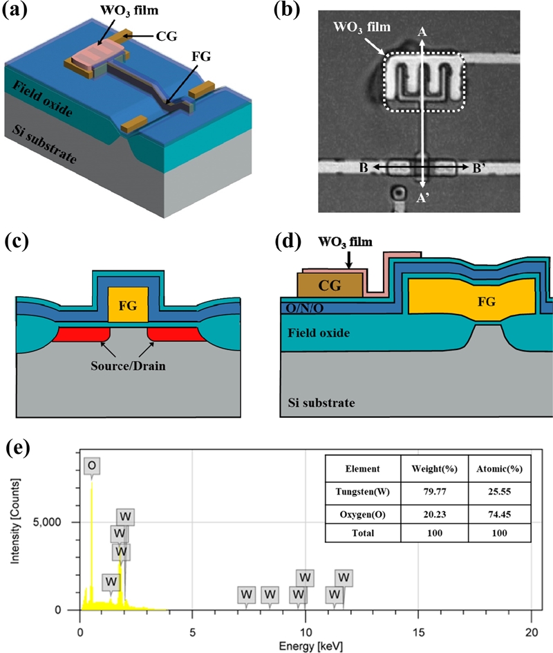
(a) Schematic bird’s eye view and (b) Microscopic image of the FET-type gas sensor with the WO3 sensing layer. (c) and (d) Cross sectional view cut along the line A-A’ and B-B’ in (b) respectively. (e) EDS spectrum of the deposited WO3 sensing material.
The WO3 film is deposited using an RF magnetron sputtering method at 20°C, using radio frequency (RF) magnetron sputtering method. The RF power, working pressure, and rate of flow of argon (Ar) gas are 150 W, 10 mTorr, and 30 sccm, respectively. The thickness of the WO3 sensing layer is varied from 100 nm to 1μm by changing the deposition time from 7 min to 70 min during the sputtering process. Finally, the PR is removed using the lift-off method, leaving only the WO3 sensing layer. As indicated by the white dashed line in Fig. 1 (b), the WO3 sensing layer is well deposited on the interdigitated FG-CG area. Energy dispersive X-ray spectroscopy (EDS) (Fig. 1 (e)) is conducted to confirm the composition of the WO3 sensing layer. The results of the EDS confirm the presence and appropriate composition of tungsten (W) and oxide (O) elements in the sensing layer. The table in Fig. 1 (e) depicts the weight and atomic concentration of the two elements.
3. RESULTS AND DISCUSSIONS
3.1 Gas response at different operating temperatures and NO2 concentrations
Figs. 2 (a) and (b) depict the transfer characteristics (ID-VCG and ID-VDS, respectively) of the fabricated FET-type gas sensor. Both the width and length of the sensor are 2 μm. And VDS is fixed at -0.1 V and the on-/off- current ratio (Ion/Ioff) at 20°C is approximately 107. As depicted in fig 2 (a), Ioff increases with an increase in the operating temperature, because at higher operating temperatures, a leakage current occurs at the junction of the source/drain and the substrate [15].
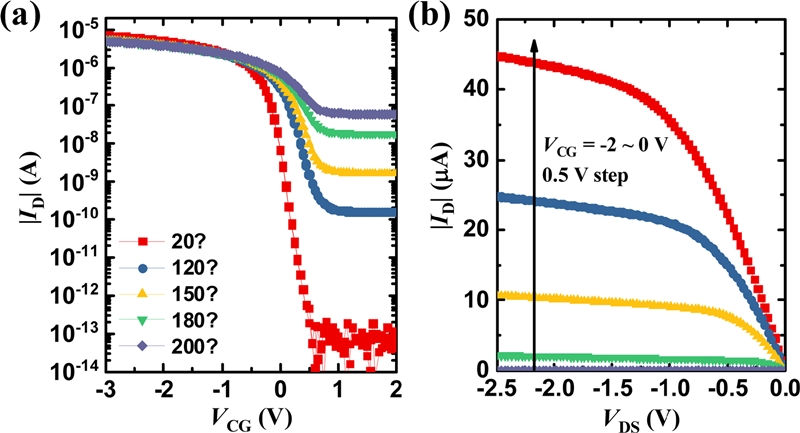
(a) Transfer characteristics (ID-VCG) of the FET-type gas sensor having the WO3 film with different operating temperatures and (b) ID-VD of the FET-type gas sensor at RT.
The sensing mechanism in which WO3 reacts with NO2 gas is explained as follows. On getting exposed to NO2 gas, the WO3 sensing layer reacts with the NO2 gas, which attract electrons from the sensing layer [16-17]. Negatively ionized gas molecules create depletion regions in the n-type sensing material and act as equivalent oxide charges. As a result, the threshold voltage of the pFET-type gas sensor decreases, and its drain current increases, as depicted in Figs. 3 (a) and (b). The Fig. 3 (a) depicts the transient response of the gas sensor, with a 1 μm thick WO3 sensing layer, at different operating temperatures ranging between 120°C and 200°C, in a 500 ppb NO2 gas atmosphere. The response and recovery of the gas sensor increase with an increase in the operating temperature due to the faster adsorption and desorption of the gas molecules at higher operating temperature [9]. However, the reaction is limited by the diffusion rate of the gas molecules and the desorption rate of the gas molecules also decreases at high temperatures [18-19]. Therefore, the rate of response begins to decrease beyond a certain temperature. In this study, an optimum temperature of 180°C is employed, considering both the response and recovery rates of the gas sensor. At this optimum temperature, we confirm the response and recovery characteristics of the sensor. At 180°C, the time to reach 90% of the sensor’s maximum response point is 53s after the injection of NO2 gas. And the time to reach 90% of the sensor’s maximum recovery point is 63 s after the injection of the reference gas for recovery. Fig. 3 (b) depicts the transient response of the gas sensor, with a 1 μm thick WO3 sensing layer, at NO2 concentrations ranging between 125 ppb and 500 ppb, and at a temperature at which the gas sensor demonstrates an optimal performance, i.e., 180°C. The rate of the response of the gas sensor increases from 56% to 138% with an increase in the concentration of the NO2 gas from 125 to 500 ppb.
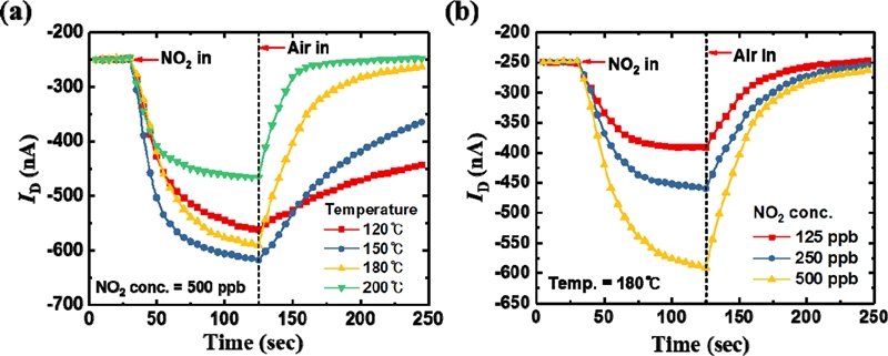
Transient response of the FET-type gas sensor with a 1 μm thick WO3 sensing layer (a) at operating temperatures ranging between 120°C and 200°C in 500 ppb NO2 atmosphere, and (b) at NO2 concentrations ranging between 125 ppb and 500 ppb at 180°C.
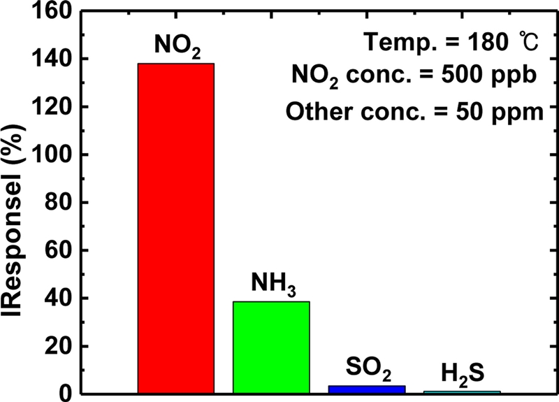
Fig. 4 illustrates a comparison of the response targeting to the four other gases (NO2, NH3, SO2, and H2S) at 180°C. The concentrations of the other three gases (NH3, SO2, and H2S) are 50 ppm and the concentration of the NO2 gas is 500 ppb. As depicted in Fig. 4, the response of the sensor is much better than that of other gases although the concentration of the NO2 gas is lower than that of other gases. Therefore, we confirm the gas sensor has significantly good selectivity for NO2 gas.
3.3 Gas response with different WO3 thickness
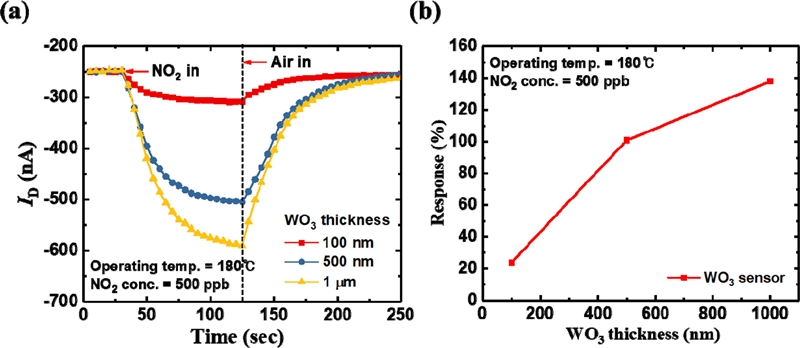
Fig. 5 depicts the transient response of gas sensors with different thicknesses of the WO3 sensing layer, ranging from 100 nm to 1 μm. The transient response is measured repeatedly, under the same NO2 gas ambience (500 ppb) and temperature (180°C) conditions. As depicted in Fig. 5, the drain current remains the same in each measurement cycle. The gas sensors are fully recovered for the recovery time of 130 s regardless of the thickness of the sensing layer. Fig. 6 (a) and (b) depict the transient response of the gas sensors with different thicknesses of the sensing layer. The gas sensors with 100 nm, 500 nm, and 1 μm thick sensing layers have 24, 101, and 138 % responses at a 500 ppb NO2 gas concentration, respectively. These results demonstrate that the response increases as the thickness of the sputtered WO3 film increases. As reported in previous work, sputtered WO3 film consists of a dense part and porous part [20]. The area of the porous part of the WO3 film increases as the thickness of the film increases. The increased area of the porous part of the WO3 film promotes the reaction of the sensing layer with the NO2 gas molecules [21-22]. Consequently, the drain current change (response) of the FET-type gas sensor increase as the thickness of the sensing layer increases.
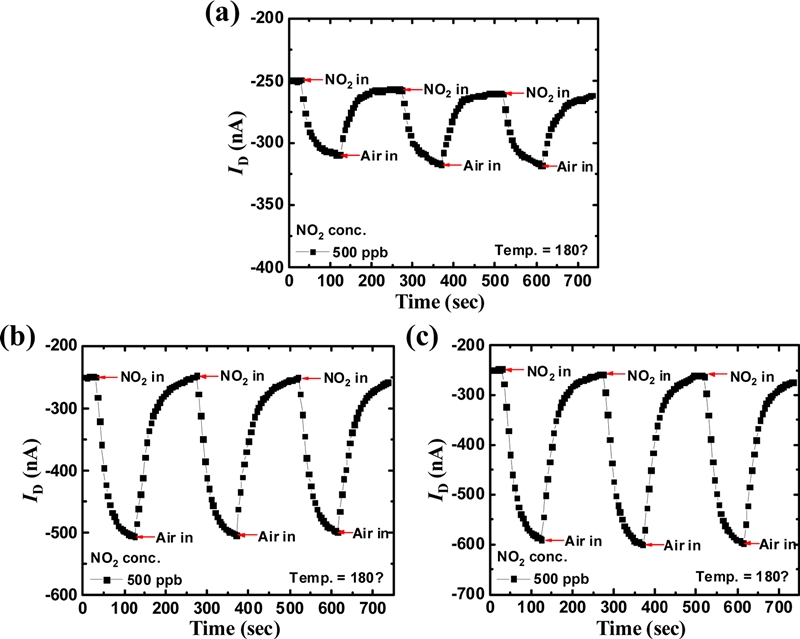
(a) Transient response to 500 ppb NO2 of the FET-type gas sensor having different WO3 thickness in the range of (b) 100 nm, (c) 500 nm, and (d) 1 μm.
4. CONCLUSIONS
In this study, we investigated the NO2 gas sensing characteristics of a Si MOSFET gas sensor with the WO3 sensing layer. The gas sensor used in this study consists of a horizontal FG interdigitated with CG. The WO3 sensing layer of the gas sensor is deposited on the interdigitated FG-CG by the RF magnetron sputtering method. The thickness of the sensing layer ranges between 100 nm and 1 μm. The gas sensor exhibits an optimal performance at 180°C considering the response and recovery rates with the operating temperature. The response increases from 24% to 138% as the thickness of the sensing layer increases from 100 nm to 1 μm. This study provides information on the operating temperature and, process conditions of the sensing material in an FET-type gas sensor with WO3 sensing material including the porous layer.
Acknowledgments
This work was supported by the National Research Foundation of Korea (NRF-2016R1A2B3009361) and the Brain Korea 21 Project in 2019.
References
-
O. S. Wolfbeis, “Fiber-optic chemical sensors and biosensors”, Anal. Chem., Vol. 76, No. 12, pp. 3269-3284, 2004.
[https://doi.org/10.1021/ac040049d]

-
J. Hodgkinson, and R. P. Tatam, “Optical gas sensing: a review”, Meas. Sci. Technol., Vol. 24, No. 1, pp. 012004(1)-012004(59), 2012.
[https://doi.org/10.1088/0957-0233/24/1/012004]

- Z. Yunusa, M. N. Hamidon, A. Kaiser, and Z. Awang, “Gas sensors: A review”, Sens. Transducers, Vol. 168, No.4, pp. 61-75, 2014.
-
A. W. Hodgson, P. Jacquinot, L. R. Jordan, and P. C. Hauser, “Amperometric gas sensors of high sensitivity”, Electroanalysis, Vol. 11, No.10-11, pp. 782-787, 1999.
[https://doi.org/10.1002/(SICI)1521-4109(199907)11:10/11<782::AID-ELAN782>3.0.CO;2-S]

-
A. M. Azad, S. A. Akbar, S. G. Mhaisalkar, L. D. Birkefeld, and K. S. Goto, “Solid·state gas sensors: A review”, J. Electrochem. Soc., Vol. 139, No. 12, pp. 3690-3704, 1992.
[https://doi.org/10.1149/1.2069145]

-
S. R. Morrison, “Semiconductor gas sensors”, Sens. Actuators, Vol. 2, pp. 329-341, 1981.
[https://doi.org/10.1016/0250-6874(81)80054-6]

-
H. M. Fahad, H. Shiraki, M. Amani, C. Zhang, V. S. Hebbar, W. Gao, H. Ota, M. Hettick, D. Kiriya, Y. Z. Chen, Y. L. Chueh, and A. Javey, “Room temperature multiplexed gas sensing using chemical-sensitive 3.5-nm-thin silicon transistors”, Sci. Adv., Vol. 3, No. 3, pp. e1602557, 2017.
[https://doi.org/10.1126/sciadv.1602557]

-
C. H. Kim, I. T. Cho, J. M. Shin, K. B. Choi, J. K. Lee, and J. H. Lee, “A new gas sensor based on MOSFET having a horizontal floating-gate”, IEEE Electron Device Lett., Vol. 35, No. 2, pp. 265-267, 2013.
[https://doi.org/10.1109/LED.2013.2294722]

-
Y. Hong, C. H. Kim, J. M. Shin, K. Y. Kim, J. S. Kim, C. S. Hwang, and J. H. Lee, “Highly selective ZnO gas sensor based on MOSFET having a horizontal floating-gate”, Sens. Actuators, B, Vol. 232, pp. 653-659, 2016.
[https://doi.org/10.1016/j.snb.2016.04.010]

-
S. S. Shendage, V. L. Patil, S. A. Vanalakar, S. P. Patil, N. S. Harale, J. L. Bhosale, J. H. Kim, and P. S. Patil, “Sensitive and selective NO2 gas sensor based on WO3 nanoplates”, Sens. Actuators, B, Vol. 240, pp. 426-433, 2017.
[https://doi.org/10.1016/j.snb.2016.08.177]

-
Y. Zhao, Z. C. Feng, and Y. Liang, “Pulsed laser deposition of WO3-base film for NO2 gas sensor application”, Sens. Actuators, B, Vol. 66, No.1-3, pp. 171-173, 2000.
[https://doi.org/10.1016/S0925-4005(00)00326-9]

-
C. J. Jin, T. Yamazaki, Y. Shirai, T. Yoshizawa, T. Kikuta, N. Nakatani, and H. Takeda, “Dependence of NO2 gas sensitivity of WO3 sputtered films on film density”, Thin Solid Films, Vol. 474, No. 1-2, pp. 255-260, 2005.
[https://doi.org/10.1016/j.tsf.2004.09.009]

-
Y. Hong, S. Hong, D. Jang, Y. Jeong, M. Wu, G. Jung, J. H. Bae, J. S. Kim, K. S. Chang, C. B. Jeong, C. S. Hwang, B. G. Park, and J. H. Lee, “A Si FET-type Gas Sensor with Pulse-driven Localized Micro-heater for Low Power Consumption”, Proc. of IEEE Int. Electron Devices Meet., pp. 12.6.1-4, San Francisco, US, 2018.
[https://doi.org/10.1109/IEDM.2018.8614562]

-
S. Hong, Y. Hong, Y. Jeong, G. Jung, W. Shin, J. Park, J. K. Lee, D. Jang, J. H. Bae, and J. H. Lee, “Improved CO gas detection of Si MOSFET gas sensor with catalytic Pt decoration and pre-bias effect”, Sens. Actuators, B, Vol. 300, pp. 127040, 2019.
[https://doi.org/10.1016/j.snb.2019.127040]

-
P. C. Jong, G. C. M. Meijer, and A. H. M. Roermund, “A 300°C Dynamic-Feedback Instrumentation Amplifier”, IEEE J. Solid State Circuits, Vol. 33, pp. 1999-2009, 1998.
[https://doi.org/10.1109/4.735541]

-
L. G. Teoh, Y. M. Hon, J. Shieh, W. H. Lai, and M. H. Hon, “Sensitivity properties of a novel NO2 gas sensor based on mesoporous WO3 thin film”, Sens. Actuators, B, Vol. 96, No.1-2, pp. 219-225, 2003.
[https://doi.org/10.1016/S0925-4005(03)00528-8]

-
H. Xia, Y. Wang, F. Kong, S. Wang, B. Zhu, X. Guo, J. Zhang, Y. Wang, and S. Wu, “Au-doped WO3-based sensor for NO2 detection at low operating temperature”, Sens. Actuators, B, Vol. 134, No. 1, pp. 133-139, 2008.
[https://doi.org/10.1016/j.snb.2008.04.018]

-
M. A. Chougule, S. Sen, and V. B. Patil, “Fabrication of nanostructured ZnO thin film sensor for NO2 monitoring”, Ceram. Int., Vol. 38, No. 4, pp. 2685-2692, 2012.
[https://doi.org/10.1016/j.ceramint.2011.11.036]

-
C. Wang, L. Yin, L. Zhang, D. Xiang, and R. Gao, “Metal oxide gas sensors: sensitivity and influencing factors”, Sensors, Vol. 10, No. 3, pp. 2088-2106, 2010.
[https://doi.org/10.3390/s100302088]

-
Y. A. Lee, S. S. Kalanur, G. Shim, J. Park, and H. Seo, “Highly sensitive gasochromic H2 sensing by nano-columnar WO3-Pd films with surface moisture”, Sens. Actuators, B, Vol. 238, pp. 111-119, 2017.
[https://doi.org/10.1016/j.snb.2016.07.058]

-
M. Hu, J. Zeng, W. Wang, H. Chen, and Y. Qin, “Porous WO3 from anodized sputtered tungsten thin films for NO2 detection”, Appl. Surf. Sci., Vol. 258, No. 3, pp. 1062-1068, 2011
[https://doi.org/10.1016/j.apsusc.2011.09.002]

-
J. Zeng, M. Hu, W. Wang, H. Chen, and Y. Qin, “NO2-sensing properties of porous WO3 gas sensor based on anodized sputtered tungsten thin film”, Sens. Actuators, B, Vol. 161, No. 1, pp. 447-452, 2012.
[https://doi.org/10.1016/j.snb.2011.10.059]

