Lithium Niobate (LiNbO3) Photonic Electric-Field Sensors
This is an Open Access article distributed under the terms of the Creative Commons Attribution Non-Commercial License(https://creativecommons.org/licenses/by-nc/3.0/) which permits unrestricted non-commercial use, distribution, and reproduction in any medium, provided the original work is properly cited.
Abstract
This study comprehensively reviewed four types of integrated-optic electric-field sensors based on titanium diffused lithium-niobate waveguides: symmetric and asymmetric Mach-Zehnder interferometers, 1×2 directional couplers, and Y-fed balanced-bridge Mach-Zehnder interferometers. First, we briefly explain the crystal properties and electro-optic effect of lithium niobate and the waveguide fabrication process. We theoretically analyzed the key parameters and operating principles of each sensor and antennas. We also describe and compare the design, simulation, implementation, and performance tests: dc and ac characteristics, frequency response, dynamic range, and sensitivity. The experimental results revealed that the sensitivity of the sensor based on the Y-fed balanced bridge Mach-Zehnder interferometer (YBB-MZI) was higher than that of the other types of sensors.
Keywords:
Integrated-optic electric-field sensor, Electro-optic effect, Lithium niobate (LiNbO3), Titanium diffused channel waveguide, Mach-Zehnder interferometer, 1×2 directional coupler, Y-fed balanced bridge Mach-Zehnder interferometer (YBB-MZI), Dipole patch antenna1. INTRODUCTION
The role and necessity of electric-field sensors in a variety of scientific and applied technology fields have steadily increased, including static and dynamic electric-field measurements in power equipment, generation and distribution of electric power [1-3], communication equipment and antennas [4], medical applications and electromagnetic compatibility (EMC) [5-7]. Electric-field sensors with broad and flat frequency responses are important tools for accurately determining the EM field distribution, particularly in EMC/EMI applications involving transient or pulsed electric-fields [8, 9]. Based on these potential applications, the requirements for electric-field sensors are as follows: wide frequency bandwidth, large dynamic range, high spatial resolution, minimal interference to the original field, and high stability and accuracy.
Conventional electric-field sensors typically use conductive parts that can interfere with the field to be measured and are very sensitive to electromagnetic noise. Also, frequency bandwidth limitations and a 50-Ω characteristic impedance in the case of radio frequency (RF) waveguides limit the scope of applicability of such technology.
Photonic electric-field sensors—being all-dielectric—present several intrinsic advantages compared to their metallic counterparts, such as noise immunity, low dispersion, wide bandwidth, minimal perturbation of the electric-field, feasibility of electrode-free operation, and—consequently—the possibility of operating even in harsh or dangerous environments. They can position the sensor at a long distance from the readout system through an optical fiber cable. We located the optical source and detector remotely to avoid perturbation of the measured field. [10,11]
The rapid development of electro-optic technologies has led to the manufacturing of compact electric-field photonic sensors based on integrated optic technology. Also, a battery does not limit the operating time. The length of the externally expanded receiving antenna—connected to the electrodes of the electrooptical modulator—determines the dimensions of this sensor type. To reduce the overall size of the sensor, we integrated a receiving dipole patch antenna into the electro-optic substrate by using a combined antenna–modulator structure [12-18].
Ti:LiNbO3 photonic modulators for electric-field sensing are classified into three types according to differences in their waveguide configurations and operation principles: symmetric [19-21] and asymmetric [22-25] Mach-Zehnder interferometers (s-MZIs and a-MZIs, respectively), 1×2 directional couplers (DC) [26-32], and Y-fed balanced bridge Mach-Zehnder interferometers (YBB-MZIs) [33-38]. The optical channel waveguide can be fabricated on a LiNbO3 substrate through titanium (Ti) in-diffusion, with co-planar antenna/electrodes located along the waveguide by photolithography. Of course, because no certain type of photonic modulator can perform well over the entire range of electric-field strengths, frequency responses, and sensitivities, the design details must be optimized for specific applications.
In this paper, we review and compare the Ti:LiNbO3 electric-field photonic sensors that have been designed, implemented, and tested in our laboratory. Section 2 describes the lithium-niobate crystal properties, including the electro-optic effect and the detailed fabrication process of the titanium-diffused channel waveguide [39, 40]. We review the operating principles of the four types of sensors, and subsequently summarize the experimental measurement results of each sensor—such as dc/ac characteristics, RF spectra, frequency responses, and sensitivity—in successive sections, with their performances compared with each other. In the final section, we summarize the conclusions of the chapter and discuss the outlook for the future
2. OPTICAL PROPERTIES OF LITHIUM NIOBATE AND WAVEGUIDES
2.1 Properties of Lithium Niobate
Lithium niobate is one of a ferroelectric crystalline oxide material with strong second-order nonlinearity [41]. One reason for the dominance of lithium niobate over lithium tantalate (LiTaO3 [42]) in photonics is its higher Curie temperature, which enables it to withstand higher processing temperatures during waveguide fabrication. Lithium niobate belongs to the trigonal crystal system, which means that its unit cell resembles a cube that has been stretched along the body diagonal. Its crystallographic group at 3m means that it has a single threefold rotational symmetry axis with a mirror plane. Therefore, this is referred to as a uniaxial crystal [43].
The axis of rotational symmetry—designated as the c-axis, z-axis, or optical axis—has a crucial impact on the optical properties because it is responsible for the birefringence of the material. That is, light polarized parallel to the optical axis refracts differently than light polarized in the plane perpendicular to that axis [39]. As a result, only two independent indices of refraction are termed the ordinary (no) and extraordinary (ne) indices, respectively. The optical axis plays another crucial role in device engineering because the permanent dipole moment or spontaneous polarization is parallel to that axis, and reversing spontaneous polarization changes the sign of the key nonlinear optical and electro-optical coefficients [44].
In early nonlinear-optic experiments with LiNbO3, researchers observed a degradation of optical properties—that is, spatial variation of the refractive index—at high optical power densities, particularly at visible wavelengths, known as the photorefractive effect or damage [43]. The trapping of photo-generated charge carriers causes the photorefractive effect, resulting in a space charge distribution that produces an inhomogeneous electric-field in the crystal. This field then generates refractive-index variations through the electro-optic effect, which is more pronounced at shorter wavelengths, where photons have sufficient energy to generate mobile charge carriers. The photorefractive effect developed into a useful mechanism for holographic recording, and specially doped crystals such as Fe:LiNbO3 have been grown to enhance photorefractive sensitivity [44]. Doping with Mg and Zn has been found to reduce the photorefractive sensitivity of lithium niobate by eliminating Nb anti-site defects that serve as electron traps [45].
2.2 Electro-Optic Effect of LiNbO3
The electro-optic effect is the change in the refractive index of a material in response to an external electric-field. [46] By using tensor notation, we can generally write the change in the refractive index, Δnij because of applied fields of Ek,1 as
| (1) |
in which γijk and Rijkl are the linear (Pockel’s effect) and quadratic (Kerr effect) electro-optic tensor coefficients, and each of the subscripts (i, j, and k) can be any one of the orthogonal crystal physics axes defined in the unit cell of each material. Upon further simplification, we obtain: the following:
| (2) |
The linear electro-optic effect is a change in the refractive indices of the normal modes of propagation—that is, ordinary and extraordinary modes in uniaxial crystals—caused by and is proportional to the applied electric-field. This effect exists only in crystals that do not possess inversion symmetry (centrosymmetric crystals). The structures of these crystals remained invariant during the inversion operation. Because ferroelectrics are polar, non-centrosymmetric, and exhibit a first-order tensor property, they also exhibit a linear electro-optic effect. The linear change in the electro-optic tensor of LiNbO3 because of arbitrary electric-fields (Ex Ey Ez) can be expressed in a 6×3 matrix form as follows:
| (3) |
By using contracted notation, the index ellipsoid in the presence of an applied electric-field can be written as
| (4) |
The largest and most useful linear electro-optic coefficient in LiNbO3 is the component, which is approximately 32.5 pm/V. An external electric-field in the 3 corresponding to the c-axis or z-axis direction gives rise to a change in the n3 index (ne or extraordinary index), as well as a change in the ordinary refractive index n1=n2 (the ordinary index, no) as given by the following:
| (5-1) |
| (5-2) |
2.3 Fabrication of Ti Diffused Lithium Niobate Optical Waveguide
Lithium niobate optical waveguides allow full usage of the material’s ferroelectric, electro-optic, and acousto-optic potentials, which provide an ideal platform for low-loss, linear, and nonlinear integrated guided wave devices. The established method of fabricating waveguides in lithium niobate—the in-diffusion of dopants—increases the refractive index [47,48] Because the dopant concentration—and, therefore, the refractive index profile—is non-uniform, diffused waveguides fall into the general category of graded index (GRIN) media. Ti ions and protons are the most commonly used dopants. Zn is sometimes used in high-power applications [28].
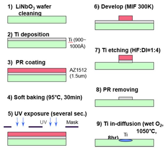
Fig. 1 shows the overall fabrication process of titanium diffused lithium niobate channel waveguide. Titanium in-diffusion is the most commonly used method for producing waveguides in LiNbO3, with depositing 300-1050 Å thickness layer of titanium on the surface by RF sputtering or e-beam evaporation as a first step. The lay thickness mostly depends on the light wavelength for single mode propagation. On top of the titanium layer, we used a spin coater to deposit a photoresist of 1 μm thickness. After baking the photoresist, we used a mask aligner for contact imprinting the desired structure patterns into the resist layer. The developed photoresist structure acts as protection mask for the subsequent etching process of the titanium layer. The etched Ti-structures are stripes which define the guiding channels after in-diffusion.
To ensure the homogeneity of Ti:LiNbO3 waveguides, the photo-lithographically defined Ti-stripes must be homogeneous in width and height. Then we placed the substrate in a diffusion furnace at about 1025-1050oC and heated it in a flowing gas atmosphere containing oxygen. For example, argon or oxygen, which has been through an H2O bubbler, is often used. As we moved the Ti coated LiNbO3 substrate into the furnace, oxidation of the deposited Ti began when its temperature reaches about 500oC. By the time the substrate has reached the desired diffusion temperature set somewhere in the range of 1025-1050oC, oxidation was complete and the Ti metal was replaced by a layer of polycrystalline TiO2. This TiO2 subsequently reacts with the LiNbO3 to form a complex compound at the surface, which acts as the diffusion source of Ti atoms.
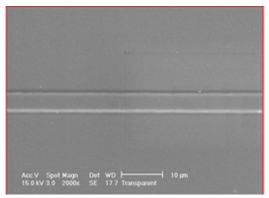
The extent of Ti diffusion depends on the diffusion coefficient, time, and temperature. It follows the usual Fick’s laws for diffusion from a limit source of atoms yielding a Gaussian distribution of diffused Ti atoms as a function of depth from the surface [39]. The advantage of this multi-staged diffusion process—as compared to diffusion directly from a metallic Ti layer—is the prevention of the out-diffusion of Li atoms from the LiNbO3. Li out-diffusion would otherwise result in changes in the index of refraction to a much greater depth than that desired for single mode waveguides. With the oxidation process, the change in index occurs only over the depth of the diffused Ti profile, which is accurately controllable. The local Ti-concentration leads to an increase of ordinary and extraordinary refractive index. Therefore, Ti:LiNbO3 waveguides allow guiding in both TE- and TM polarization modes. Fig. 2 shows the top-view optical micrograph of titanium stripe in-diffused waveguide.
3. ELECTRIC-FIELD SENSORS WITH MACH-ZEHNDER INTERFEROMETER (MZI)
One sensing scheme that has received the most attention in the area of photonic electric-field sensors is the Mach-Zehnder interferometer, based on an integrated-optic titanium-diffused optical channel waveguide. Therefore, this section first addresses two configurations: symmetric and asymmetric. The former, using a push-pull lumped electrode and plate-type probe antenna with a wide effective area, is more useful than one with a dipole antenna to measure the relatively low-frequency electric-field strength. The latter, with two arms with a length difference of a quarter wavelength, is designed to achieve the π/2 phase difference [22].
3.1 Symmetric Mach-Zehnder Interferometer (s-MZI)
Fig. 3(a) shows the configuration of the electro-optic sensor. The optical waveguide circuit is a lumped-type symmetric Ti:LiNbO3 Mach-Zehnder interferometer [21]. The device consists of a 3-dB input splitter, an output combiner, and two straight channel waveguides. Because lithium niobate devices are polarization sensitive, the connection from the optical source to the device uses a polarization-maintaining fiber, whereas the return connection uses an ordinary single-mode fiber. The detected electric-field produces equal and opposite phase shifts in the light beam propagating in the two parallel-channel waveguides, thereby leading to a net phase shift of twice the phase shift for each channel. When the two light beams recombine at the output combiner, phase modulation converts to amplitude-modulated light at the same frequency as the electric-field. Therefore, the amplitude of the light signal is proportional to the intensity of the electric-field.
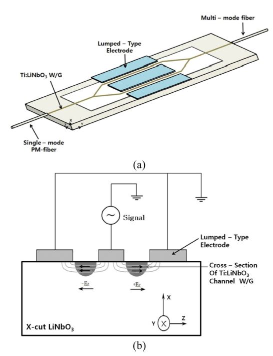
Schematic diagram of a symmetric Mach-Zehnder interferometer with metal planar electrode: (a) perspective view of the electrode placement along the channel waveguides and crystal orientation, and (b) cross-section through the interferometer arms showing the electric-field generated by a voltage applied to the electrode.
In the electrode structure on the device shown in Fig. 3(b), the induced voltage because of the detected electric-field produces an electric-field Ez along the Z-axis direction, which crosses the channel waveguides. This Z-directed electric-field interacts with the light beam propagating in the channel waveguide to produce an electro-optic modulation. The polarization of the light wave propagating in the channel waveguide should also be oriented in the Z-direction—that is, along the optical axis—which is referred to as the transverse electric (TE) mode (also called the extraordinary mode). Therefore, the oriented electric-field modifies the extraordinary refractive index ne of the substrate through the linear electro-optic effect, which is given by
| (6) |
in which is the electro-optic coefficient of lithium niobate and Γ (0 < Γ < 1) accounts for the numerical degree of the mutual overlap interaction between the applied electric-field and the optical field in the channel waveguides. The corresponding phase change in the light beam propagating in each arm is given by
| (7) |
in which λ is the wavelength of the light and L is the electrode length. We oriented the electrodes so that the electric-field through each arm has opposite polarity; therefore, we added two phase changes to determine the net phase difference when the optical signals recombine at the output. In terms of the induced voltage V and the electrode gap g, the total phase change at the output combiner is as follows:
| (8) |
In Eq. (8), the half-wave field intensity Eπ is defined as
| (9) |
We converted the phase shift produced by the electric-field in each arm to amplitude–intensity modulation at the combiner of the interferometer. The optical power transfer function of the device is expressed as
| (10) |
in which ΔΦ is the net accumulated phase difference between the arms and is generally composed of two terms: ΔΦ=Φo+ΔΦt(E). The inherent phase difference Φo is caused by the physical channel length difference or effective refractive index difference between the two channel waveguides. The second term, ΔΦt(E), depends on the electric-field, as shown in Eq. (8). A linear response to the electric-field can be obtained by setting the phase bias to Φo= π/2 and operating with a small phase change ΔΦt(E) ≪1. By substituting these conditions into Eq. (10), we can obtain an output power that is almost linearly proportional to the electric-field intensity expressed in Eq. (11):
| (11) |
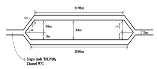
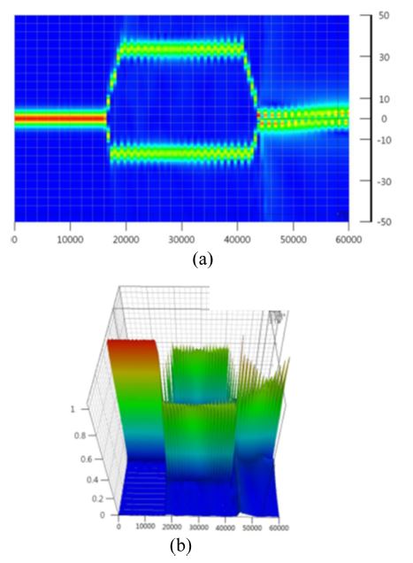
We designed a single-mode channel waveguide symmetric interferometer with lumped electrodes for operation at 1.3 μm wavelength in an X-cut, Y-propagating LiNbO3 substrate (46×7×1 mm), as shown in Fig. 4(a) which demonstrates the dimensions and arrangement of the lumped electrode structure. The interferometer had a 7.5 μm channel width, a total branching angle of 1.2°, 25 mm straight arm length, and an arm separation of 26 μm. Fig. 4(b-c) shows the BPM-CAD simulation results of the light wave propagation for the interferometer. [49] Notice that the incident light splits and combines almost equally at the input and output Y-branches, respectively.
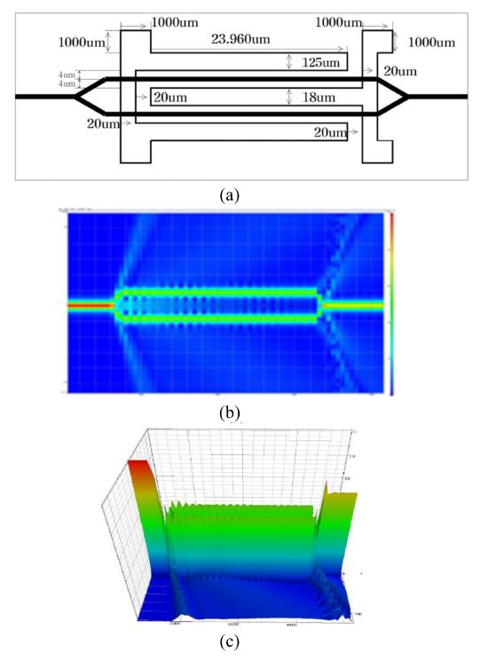
(a) Design layout and dimensions of electrodes. (b) Two-dimensional and (c) three-dimensional BPM-CAD simulation results.
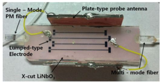
We used a standard photolithographic technique to fabricate the Mach-Zehnder interferometer modulators on X-cut LiNbO3 substrates, as explained in the previous section. Also, we fabricated 3500 Å-thick aluminum lumped electrodes to allow the sensing of the electric-field. We attached polarization-maintaining single-mode and multi-mode optical fibers to the input and output waveguides, respectively. Finally, we attached a 20 × 10 mm plate-type external probe antenna made of copper to the electrode on the substrate. Fig. 5 shows a photograph of the fabricated device with attached optical fibers and a copper plate-type antenna.
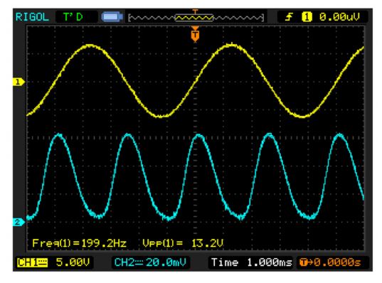
We first tested the device without attached fibers at a low frequency of 200 Hz. By using butt-coupling from a pigtailed tunable laser, we carried out the performance characterization at 1.3 μm wavelength. We butt-coupled TE-polarized light from the pigtailed tunable laser into the devices and collected the output by using a microscope objective and focusing onto a photodetector for characterization. We selected the TE or TM input polarization by proper adjustment of the fiber-polarization controller. In the interferometers, we observed single-mode propagation of TE polarization. To measure the modulation depth and half-wave voltage Vπ, we applied a sinusoidal voltage signal sufficiently large to drive the device output between the maximum and minimum.
Fig. 6 shows oscilloscope traces of a 200 Hz sinusoidal voltage drive signal and the response as measured by the photodetector. The device has a 25 mm electrode length and a 15.5 μm gap. It exhibited the modulation depths of almost 100 % and a Vπ voltage of 6.6 V at modulation frequencies of 200 Hz.
We performed frequency tests to evaluate the minimum detectable field and the frequency response of the fiber-coupled sensor. The incident optical power was of the order of 14 mW. Fig. 7 shows the block diagram of the experimental setup. We tested the device in a uniform electric-field by placing it in a TEM cell (TescomTC-5010A), as shown in Fig. 7. [50] We fed the optical fibers through the sloping walls of the TEM cell and connected them to the laser and photodetector via FC/PC fiber optic connectors. The 20−-20 dBm (100 mW−10 μW) RF input to the TEM cell corresponds to an electric-field strength from 0.293 to 23.2 V/m. The RF power travels through the TEM cell in the same direction as the propagation of light in the optical fibers and sensor.
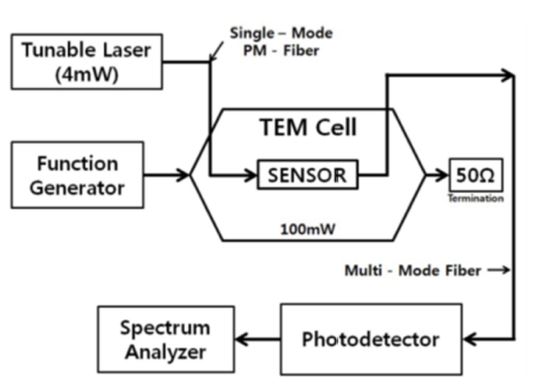
Block diagram of the test setup for the measurement of electric-field sensing and the evaluation of the frequency response.
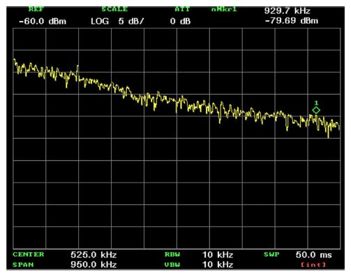
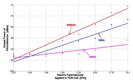
Fig. 8 shows the spectrum analyzer outputs for a 20 dBm input to the TEM cell at frequencies of 500 KHz, 1 MHz, and 5 MHz. We measured the RF powers received at the photo detector at -0.66, -76.58, and -86.72 dBm at the applied RF frequencies, respectively. Therefore, we obtained the frequency response of the sensor in a TEM cell, as shown in Fig. 9. The 0.66 V/m field across the sensor would cause a peak phase difference of ΔΦt(E) =6.72×10⁻⁶ radians, according to Eq. (8). Fig. 8 shows the signal powers measured at about -92.41, -93.38, and -92.83 dBm, with the noise floor at about 70.66, -76.58, and -86.72 dBm at frequencies 500 KHz, 1 MHz, and 5 MHz, respectively. Therefore, the internal electric-field of 23.2 V/m in the TEM cell produces signal-to-noise ratio (SNR) of 22, 17, and 6 dB, respectively, at these frequencies. The minimum detectable electric-field is 1.84, 3.28, and 11.6 V/m, based on the Emin = 23.2 × 10(-SNR/20). Fig. 10 shows the sensitivity curves at the frequencies of 500 KHz, 1 MHz, and 5 MHz. The sensor exhibits a linear-like response tendency for an applied electric-field intensity from 0.293 to 23.2 V/m.
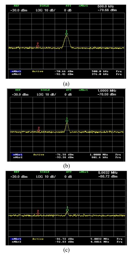
The RF responses of sensor to (a) a 500 KHz, (b) 1 MHz, and (c) 5 MHz RF input signal of a 100 mW power into the TEM cell.
3.2 Asymmetric Mach-Zehnder Interfermeter (a-MZI)
Fig. 11(a-b) shows the configuration of the asymmetric Ti:LiNbO3 Mach–Zehnder interferometer with an electrode and dipole antenna. [22] We designed the device to have a π/2 phase difference between its two arms by adjusting the path length difference, which improves the linearity and sensitivity of the sensor without external bias. The voltage induced by the sensing electric-field produces phase shifts in the light beam propagating in one of the parallel channel waveguides, thereby leading to a net phase shift between the two light beams through each channel. When the two light beams recombine at the output combiner, phase modulation converts to an amplitude-modulated signal at the same frequency as the induced signal voltage. Therefore, the amplitude of the light signal is proportional to the sensing electric-field.
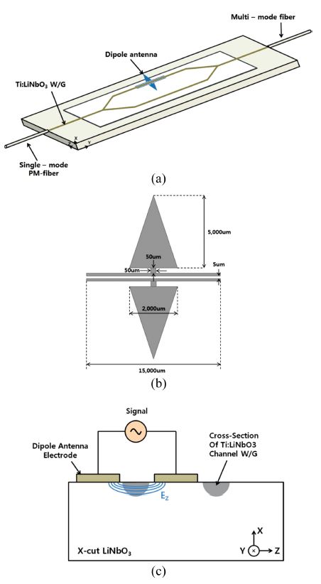
(a) Schematic diagram of asymmetric Mach–Zehnder interferometer with a dipole antenna, (b) structure and dimensions of dipole antenna, and (c) cross-section through the interferometer arms showing the electric-field generated by a voltage applied to the dipole antenna.
In the electrode structure of the device shown in Fig. 11(c), the applied signal voltage produces an electric-field Ez along the z-axis direction. This electric-field generated by the applied voltage modifies the extraordinary refractive index ne of the substrate through the linear electro-optic effect, which is given by Eq. (6) and defined in the symmetric MZI. The corresponding phase change in the light beam propagating in the arm with a dipole antenna is given by
| (12) |
in which λ is the wavelength of light, L is the electrode length, and Eπ is the half-wave field, which is defined as
| (13) |
Comparing Eqs. (8), (9), (12), and (13) shows a difference in the value of factor “2” in the numerator and denominator. This is because we applied a push-pull electrode structure to the device corresponding to the former equations, and compared to the latter, the phase change increased by 2 times. We converted the phase shift produced by the electric-field in one of the arms to amplitude-intensity modulation at the combiner of the interferometer. The optical power transfer function of the device is expressed as follows:
| (14) |
In Eq. (14), ΔΦ is the net accumulated phase difference between the arms and is composed of two terms ΔΦ = Φo + ΔΦt(E). The intrinsic phase difference Φo is caused by the difference in the physical path length and the effective refractive index between the two channel waveguides. A linear response to the electric-field can be obtained by setting the phase bias to Φo = π/2 and operating it with a small phase change (Δϕt(E) « 1). Substituting these conditions into Eq. (14) gives a device output that is linearly proportional to the electric-field:
| (15) |
We designed the asymmetric Mach-Zehnder interferometer for operation at 1.3 μm in an X-cut, Y-propagating LiNbO3 substrate, as shown in Fig. 12. The channel width, separation, and branching angle of the asymmetric Mach-Zehnder interferer were the same as those presented in Section 3.1.1. However, we obtained a phase difference of π/2 between the light waves that propagated through the two channels by adjusting the channel length through geometric analysis.
We designed the optical path difference ΔL by adjusting where one interferometer channel waveguide was extended by ΔL relative to the other. Then ϕo is given by
| (16) |
in which κ = λ⁄2π and neff are the effective refractive indices of the optical modes in the waveguide: at λ=1.3 μm, ΔL≈148 Å. For the configuration shown in Fig. 12, in which the input and output branches are identical, ΔL is defined as follows:
| (17) |
In Eq. (17), y is the incremental vertical height corresponding to the optical path difference ΔL between the input and output couplers. For the greatest accuracy in mask fabrication, the required y value requires an exact calculation. Fig. 13 shows the BPM-CAD simulation results for the interferometer. [49] The output power was almost half the value of the maximum input power because of an almost π/2 phase difference between the two channels.
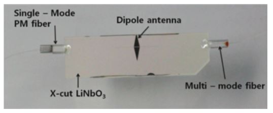
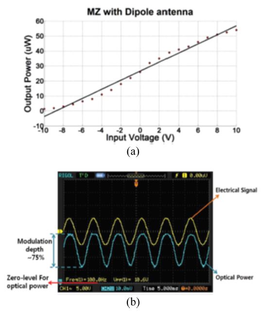
Fig. 14 shows the asymmetric device with a dipole antenna that we fabricated on an X-cut LiNbO3 substrate by using the fabrication process described in the previous section. We carried out performance characterization at a about 1.3 μm wavelength by butt-coupling from a pig-tailed tunable laser, as described in previous sections. Fig. 15(a) shows the output intensity profile of the device measured under different driving dc voltages. When no voltage was applied, the output power was almost half the value of the maximum power, corresponding to an almost π/2 phase difference between the two arms. Therefore, we intrinsically set the modulator at the 3-dB half-power point. When we increased or decreased the driving voltage, the output power of the device also changed linearly, depending on the degree of phase mismatch. Fig. 15(b) shows the ac modulation response of the device versus the driving signal voltage. The curve above in the figure shows the driving voltage signal at a frequency of 100 Hz. The asymmetric MZ modulator with a 15 mm electrode length and a 5 μm gap exhibited a modulation depth of approximately 75 % and Vπ voltage of approximately 5.3 V, as shown in Fig. 15(b). The overlap integral Г deduced from Fig. 15(b) and Eq. (3) was approximately 0.38.
We performed frequency tests to evaluate the minimum detectable field and frequency response of the fiber-coupled sensor, as described in the previous section. Fig. 16 shows the spectrum analyzer outputs for a 20 dBm input to the TEM cell at frequencies of 20, 50, and 100 MHz, respectively. We measured the RF power received at the photodetector at -89.58, -97.72, and -94.08 dBm for the fabricated device, with the noise floor at about -130 dBm at the measured frequencies, as shown in Fig. 16. The internal electric-field of 298 V/m in the TEM cell produces signal-to-noise ratios (SNRs) of 40.42, 33.28, and 35.92 dB, respectively. Therefore, the corresponding minimum detectable electric-fields were 0.28, 0.646, and 0.47 V/m.
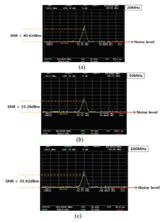
Measured RF spectrums of the fabricated sensor into the TEM cell with power level of 20 dBm: (a) 20 MHz signal, (b) 50 MHz signal, and (c) 100 MHz signal.
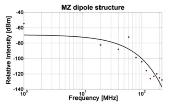
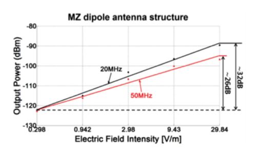
Also, we obtained the measuring frequency response of the sensor at an input RF power of 20 dBm in the TEM cell, as shown in Fig. 17. Fig. 18 shows the sensitivity curves at frequencies of 20 and 50 MHz. The sensors exhibited an almost linear response for the applied electric-field intensity from 0.298 to 29.84 V/m, corresponding to a dynamic range of approximately 32 and 26 dB at frequencies of 20 and 50 MHz, respectively.
4. SYMMETRIC 1 × 2 DIRECTIONAL COUPLER
4.1 Operation Principle
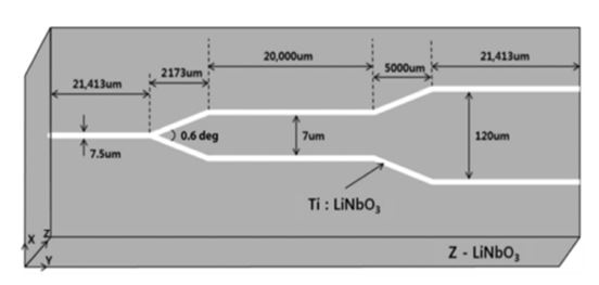
A 1×2 directional coupler modulator consists of a single-mode Y-junction splitter and co-directional coupler with two parallel and symmetric waveguide channels. [29] Fig. 19 shows the schematic diagram and its dimensions. Light that we fed into two symmetric waveguides split equally into through the Y-junction region. The co-directional coupler guides two single-mode light beams traveling along the two channels. With no modulating voltage applied, we set the coupler to the 3-dB operating point automatically because of the symmetric structure. When a driving voltage is applied through the electrodes over the coupler region, light can be coupled from one channel to another.
The 1×2 directional coupler modulator had two complementary optical outputs. In general, a 1×2 directional coupler modulator is characterized by its interaction length (L), coupling conversion length (lc), and phase mismatch of the propagation constant (Δβ) between the two arms. The phase mismatch caused by the applied voltage is calculated as
| (18) |
with each parameter defined in Section 3.1. Based on couple-mode theory, an expression for the light power output from the coupler modulator can be obtained. In a normalized condition, the light power P1 of the upper branch is expressed as
| (19) |
in which
| (20) |
with V is the normalized driving voltage, y = L/lc is the normalized interaction length, and r2 = x2 + x2. From the power conservation condition, the power in the lower branch is P2 = 1 − P1. Notice that x is a linear function of the driving voltage, although the normalized interaction length y is independent of the driving voltage. According to Eq. (19), the 1 × 2 directional coupler modulator is set at the 3-dB operation point automatically—that is, P1 = P2 = 1/2, when no driving voltage is applied.
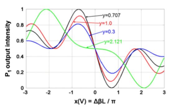
Fig. 20 shows the simulated results of the light intensity versus driving voltage with y = 0.3, 1/, 1.0, and 3⁄, respectively. Notice that the maximum modulation depths varied for different values of the interaction length. A 100% depth was reached when y = 1/ and 3⁄. Theoretically, a 100% modulation depth is possible only when L = (2n+1)/, (n= 0, 1, 2 - - ), according to Eq. (19).
4.2 Design, Simulation and Fabrication
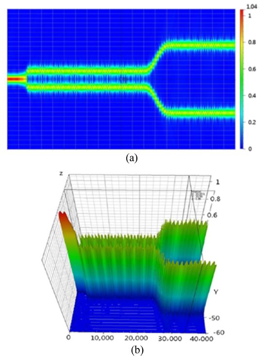
We designed a single-mode channel waveguide symmetric directional coupler with a dipole antenna for operation at 1.3 μm wavelength in a z-cut, Y-propagating LiNbO3 substrate, as shown earlier in Fig. 19. The directional coupler had a 7.5 μm channel width, a total branching angle of 0.6o, 20 mm straight arm length, and an arm separation of 7 μm. Fig. 21 shows the beam-propagation simulation (BPM-CAD) results [49]. Notice that the incident light splits almost equally at the input Y-branch.
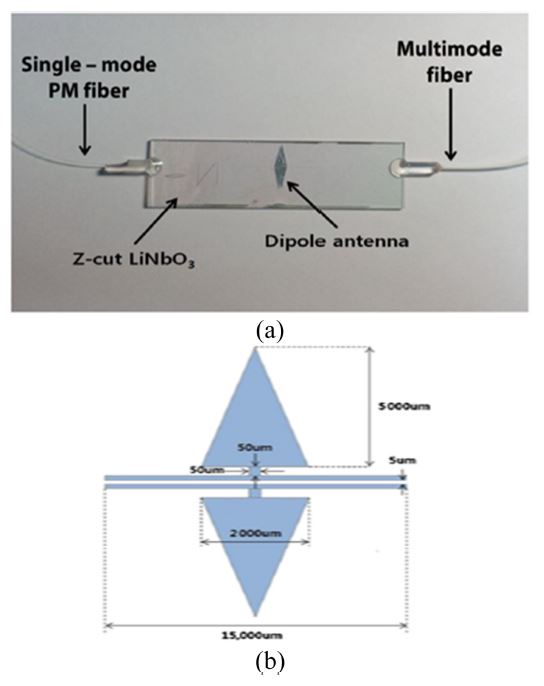
We fabricated a 1 × 2 directional coupler with a dipole antenna, as shown in Fig. 22(a), on a Z-cut LiNbO3 substrate by using the fabrication process mentioned earlier. We connected two lumped electrodes with a length of 15 mm and a gap of 5 μm to a vertical co-planar dipole antenna with a length of 5 mm, as shown in Fig. 22(b).
4.3 Measurements and Discussions
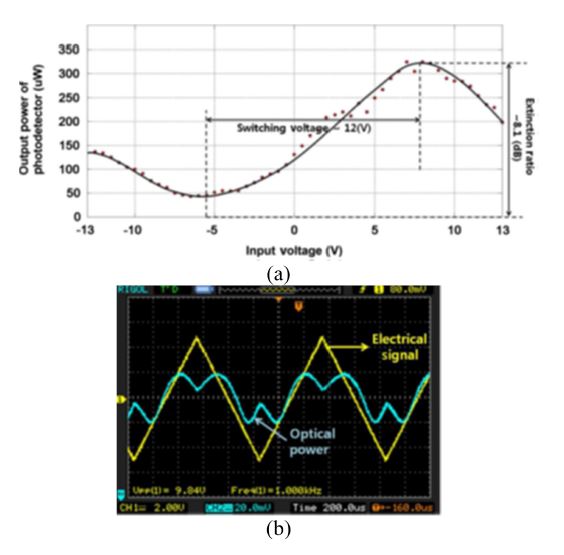
We carried out a dc performance characterization at 1.3 μm wavelength and TM polarization by butt-coupling from a pigtailed tunable laser that was collected at the output by a microscope objective and focused onto a photodetector. We observed single-mode propagation in a 1 × 2 directional coupler. When we applied no voltage, the optical output powers of the two branches were nearly identical. Therefore, we intrinsically set the modulator at approximately the 3-dB half-point. When we increased or decreased the driving voltage to 6 V, the light in one branch of the coupler modulator was coupled to the other branch, where the light output power of the former branch disappeared and the output of the latter reached a maximum.
The switching voltage applied to modulate the light power of either branch from the bar state (maximum intensity) to the cross state (minimum intensity) was 12 V, corresponding to a light extinction ratio of 8.1 dB. Fig. 23(a) shows the optical output power versus the applied voltage measured by the optical power meter. It exhibited a slightly asymmetric dc output characteristic curve and a switching voltage of 12 V. Fig. 23(b) shows the ac modulation responses of the two branches versus the driving voltage. The triangular curve in the figure represents the driving voltage signal at a frequency of 1 kHz.
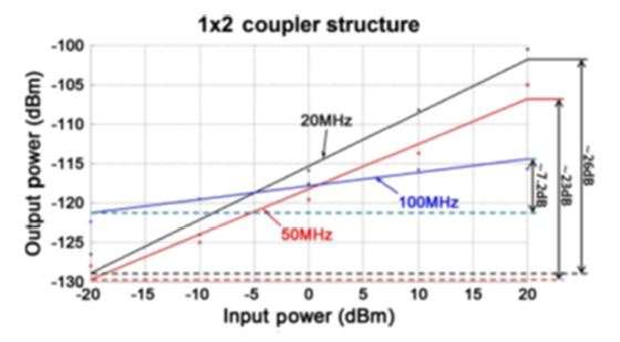
Also, we performed frequency tests to evaluate the minimum detectable field and frequency response, as described in the previous section. Fig. 24 shows the spectrum analyzer outputs for a 20 dBm input to the TEM cell at frequencies of 20 and 50 MHz, respectively. We measured the measured RF power received at the photodetector to be -100.5 and -105.05 dBm. The noise floor is approximately -130 dBm at the same frequencies. The internal electric-field of 29.8 V⁄m in TEM cell produces an SNR of about 29.5 and 25 dB, respectively, at the frequencies. Therefore, the minimum detectable electric-fields are about 0.99 and 1.67 V⁄m. Fig. 25 shows the sensitivity curves at frequencies of 20, 50, and 100 MHz. We can confirm that the graph shows almost linear response for the applied electric-field intensity from 0.293 to 23.2 V⁄m, even though some data were not on the line but very near to it. The device has dynamic ranges of approximately 26 and 23 dB at frequencies of 20 and 50 MHz, respectively. Also, we obtained the measuring frequency response of the sensor at an RF input power of 20 dBm in the TEM cell, as shown in Fig. 26.
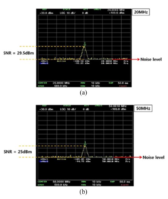
The RF spectrums of (a) 20 MHz and (b) 50 MHz RF input signal into the TEM cell with a power level of 100 mW.
5. 1 × 2 Y-FED BALANCED-BRIDGE MACH-ZEHNDER INTERFEROMETER (YBB-MZI)
5.1 Operation Principle
A 1 × 2 Y-fed balanced-bridge Mach–Zehnder interferometer modulator (1 × 2 YBB-MZI) consists of a 3-dB directional coupler at the output and has two complementary output waveguides, as shown in Fig. 27(a) [38]. We placed a dipole patch antenna around the arm of the MZI structure to detect the electric-field.
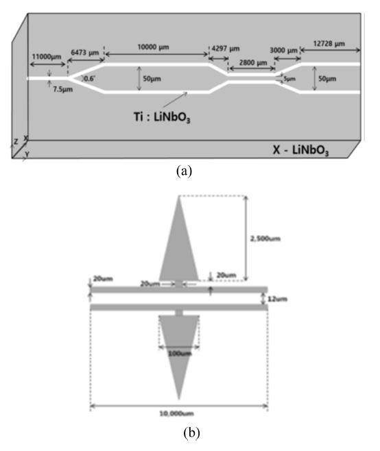
Schematic diagrams and dimensions of (a) a Ti: LiNbO3 1×2 Y-fed balanced-bridge Mach–Zehnder interferometer (YBB-MZI) and (b) a dipole patch antenna.
The coupling length Lc, coupling coefficient κ, and wavenumber β of the waveguide represents the operating characteristics of a 2 × 2 directional coupler. If we ignore the transmission loss, the transfer matrix of the directional coupler can be expressed as
| (21) |
in which Ei1, Ei2, and E01, E02 are the input and output optical modes, respectively. The incident single-mode optical wave—equally divided into two by a 3-dB power splitter located at the input stage—can be expressed as
| (22) |
in which θ is the initial phase.
The dipole patch antenna with an electrode, as shown in Fig. 27(b), creates an electric-field on one of the two arms of the MZI, which eventually induces a change in the refractive index and unbalanced modulation. Before going into the output directional coupler, the optical wave in the two arms has an extrinsic phase mismatch Φ(Ee) because of the detected electric-field. This phase mismatch Φ(Ee) can be expressed as
| (23) |
in which le is the length of the electrode connected to the dipole-patch antenna. Therefore, the optical wave entering the output coupler can be represented as
| (24-1) |
| (24-2) |
By combining (21) with (24), the output power of the YBB-MZI modulator is expressed as
| (25-1) |
| (25-2) |
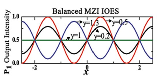
in which x = Φ(Ee) ⁄π is the normalized phase mismatch, y = Lc / lc is the normalized coupling length, and lc = π ⁄ 2k is the coupling-conversion length.
Fig. 28 shows the output intensity Po1 as simulated and plotted for the YBB-MZI electric-field sensor. The YBB-MZI sensor exhibited a sinusoidal transfer function for different y values. The value of y affects only the extinction ratio, which can be represented as sin(πy). For most cases where sin(πy)≠0, the transfer function is acceptable, as the extinction ratio affects only the E-field measurement sensitivity. To support maximum sensitivity, the coupling length should satisfy the condition as follows:
| (26) |
In Eq. (26),
5.2 Design, Simulation and Fabrication
By using single-mode Ti:LiNbO3 channel waveguides, we designed a symmetric 1 × 2 YBB-MZI modulator with a dipole patch antenna for operation at a wavelength of 1.3 μm in an x-cut, y-propagating LiNbO3 substrate, as shown earlier in Fig. 27(a). The device consists of a Y-branch splitter, phase modulator, and directional coupler. The waveguide width was 7.5 μm for single-mode operation, and the splitting angle of the Y-branch was 0.6° to decrease the propagation loss as much as possible and for fabrication tolerance. The gap interval between the two adjacent waveguides of the directional coupler and the parallel coupling length were 5 μm and 2.8 mm, respectively, to split the optical power equally into two output channels with a nominal coupling constant-length product, κ·Lc of π/4. The interval between the inner edges of the two output waveguides was 50 μm, which prevented optical power coupling between the two output channels.
As shown earlier in Fig. 27(b), the gap and length of the modulation electrode connected to the dipole patch antenna are 12 μm and 10 mm, respectively. Fig. 29 shows the results of the BPM-CAD 3D simulation of the optical wave propagating through the YBB-MZI modulator. When we applied no voltage, the two intensity profiles were approximately identical, with approximately 1% or lower accuracy because of nearly equal intensity splitting, as shown in Fig. 29(a). Therefore, we set the YBB-MZI modulator intrinsically at the 3-dB half-power point.
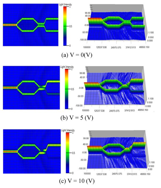
Three-dimensional BPM-CAD simulation results with the following applied voltages: (a) 0 V, (b) 5 V, and (c) 10 V.
When the driving voltage increased to 5 and 10 V, the light in the lower branch of the device coupled with the upper branch, in which the light intensity of the lower branch decreased and the intensity of the upper branch increased, as shown in Fig. 29(b). When 10 V was applied, the light of the lower branch almost disappeared, and the light intensity of the upper branch reached its highest level, as shown in Fig. 29(c). Therefore, we could theoretically confirm that the switching voltage required to modulate the light intensity of either branch from the bar state (maximum intensity) to the cross state (minimum intensity) was 10 V.
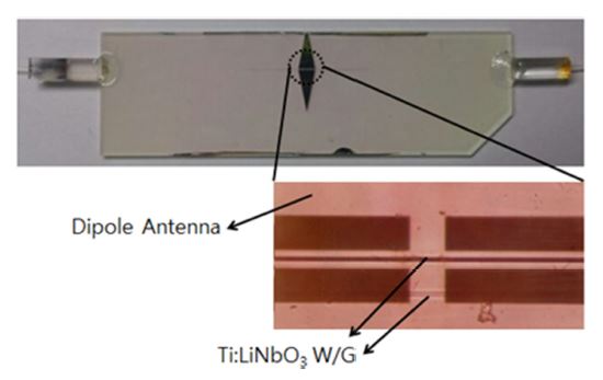
We fabricated a 1 × 2 YBB-MZI on an x-cut, 3-inch, 1-mm-thick LiNbO3 wafer, as described earlier. Fig. 30 shows a photograph of the implemented device with attached optical fibers and a dipole patch antenna. We measured the insertion loss of the device, including the input/output fiber, to be about 11.7 dB, which includes the fiber-connector loss, pig-tailing loss, mode-mismatch loss, and propagation loss of the waveguides.
5.3 Measurements and Discussions
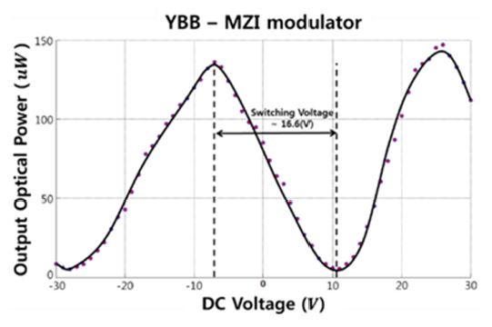
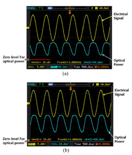
First, we tested the fabricated device without an attached optical fiber by applying a dc voltage. We used a tunable laser with butt coupling at a wavelength of 1.3 μm and TE polarization to observe the performance and characterization. Fig. 31 shows the optical output power versus the dc voltage measured by an optical power meter, a slightly asymmetric dc output characteristic, and a switching voltage of 16.6 V that corresponds to a 14.7-dB extinction ratio. We also observed that when we did not apply voltage, the two outputs of the device were almost the same. Fig. 32 shows how the ac modulation responses of the two outputs versus the driving sinusoidal voltage were further measured, with the optical signals below the sinusoidal curve and the applied ac voltage signal above the curve at a frequency of 1 kHz (5 V/div). We confirmed the power of the two outputs to be nearly equal, and the periodic exchange of the output power in the two outputs expressed a good inverse relationship in the output sinusoidal curves. We also observed a slightly skewed and flattened shape in the optical response, shown in in Fig. 32, because of the imperfect single-mode waveguide and the out-diffusion that occurred in the diffusion process.
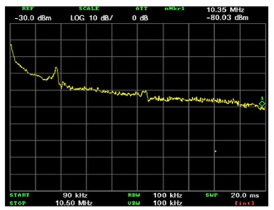
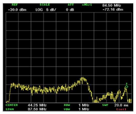
Fig. 33 shows the spectrum-analyzer outputs for an input of 20 dBm to the TEM cell at frequencies of 10, 50, and 70 MHz, respectively. We measured the RF power detected at the photodetector to be -101.5, -110.9, and -122.2, and measured the noise floor to be about -130 dBm at the same frequencies. The internal electric-field of 29.8 V/m in the TEM cell produced an SNR of 28.5, 19.1, and 7.8 dB at each frequency. Therefore, the minimum detectable electric-fields are 1.12, 3.3, and 12.13 V/m, respectively.
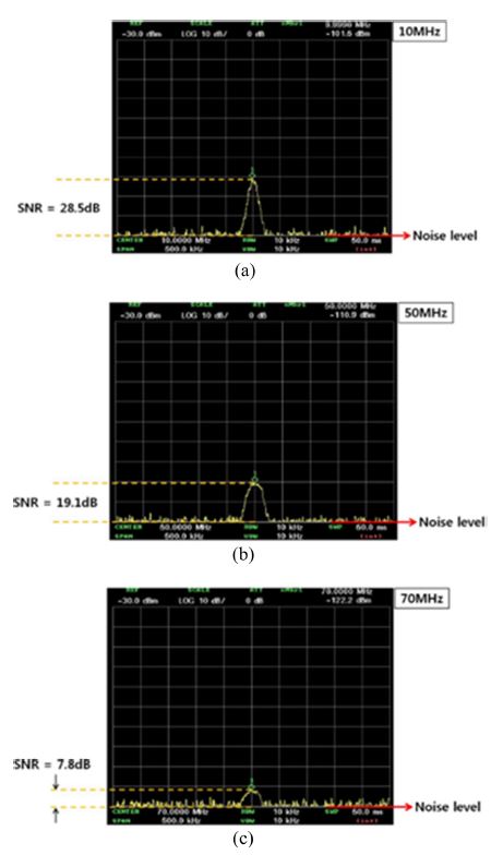
The detected RF spectra of (a) 10 MHz, (b) 50 MHz, and (c) 70 MHz RF input signals into the TEM cell, with a power level of 100 mW.
Fig. 34 shows the sensitivity curves at RF frequencies of 10, 50, and 100 MHz. We can confirm that the graph shows almost linear response characteristics from an applied electric-field intensity from 0.293 to 23.2 V/m. Although some data are off the linear response line, they remain very close. The device also shows dynamic ranges of approximately 22, 18, and 12 dB at frequencies of 10, 50, and 100 MHz, respectively. Fig. 35 shows the photodetector power at different electric-field intensities, varying the RF frequency from 10 to 100 MHz.
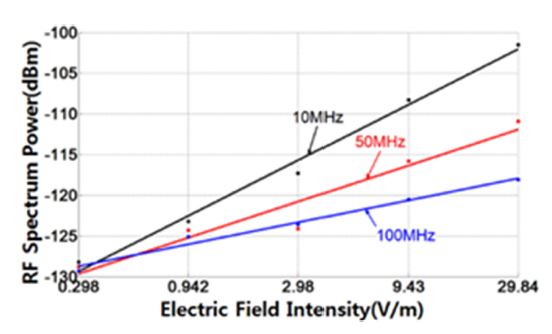
The photo-detected signal power versus the electric-field strength in the TEM cell at different frequencies.
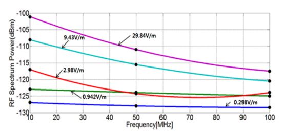
The photo-detected signal power versus frequency at different electric-field strengths in the TEM cell.
Fig. 36 shows the frequency response of the sensor measured with an 20 dBm of RF input power applied to the TEM cell, as well as a nearly flat frequency response from 1 to 50 MHz. We derived the cutoff high frequency of the device from the series-coupled time constant of the electrode resistance and the structural and packaged capacitances of the device. Therefore, a significantly higher cutoff frequency can be expected when a metal material with a higher coefficient of conductivity, such as gold instead of aluminum, is applied to an electrode.
6. CONCLUSIONS
A linear modulator that is passively biased at the optimum linear operating point is desirable for sensing the electric-field. We demonstrated this in an asymmetric MZI, directional coupler, and YBB-MZI. The first had a π/2 intrinsic bias, in which a geometric path length difference of a quarter wavelength was required between the two arms. The other two modulators—automatically biased at the optimum 3-dB operating point by a symmetrical design—offered the possibility of a more fabrication-tolerant device than the asymmetric MZI modulator. However, the transfer function of the directional coupler is complicated, and the sensor performance is unacceptable for certain specific values—that is, the ratio of the interaction length to the conversion length. In contrast, the YBB-MZI modulator uses a 3-dB coupler at the output and has two complementary output waveguides. It has a well-defined transfer function for the output optical power versus the sensed electric-field intensity and can be automatically biased at the optimum 3-dB operating point by symmetrical design, offering the possibility of a more fabrication-tolerant device than the asymmetric MZI and the 1 × 2 directional coupler.
Our theoretical analysis also confirmed that the YBB-MZI structure inherits the advantages of the asymmetric MZI and 1 × 2 directional coupler because of its sinusoidal transfer function and better optical bias control. The three sensor types exhibited an almost linear response for the applied electric-field intensity from 0.298 to 29.84 V/m.
Our experimental results confirmed that an electric-field sensor based on the YBB-MZI exhibits a superior 3-dB optical bias because of the perfect symmetry of the two arms and simple sinusoidal transfer characteristics. However, in the case of an asymmetric MZI, a 3-dB optical bias can be realized by the optical path difference between the two arms. Also, the optical bias depends on both the optical path difference and the effective refractive index of the waveguide, which is especially affected by fabrication parameters, such as titanium thickness, diffusion time, temperature, and ambience. Therefore, the YBB-MZI structure allows for a much better control of the optical bias than an asymmetrical MZI.
We reviewed four types of integrated-optic electric-field sensors based on titanium diffused lithium niobate channel waveguides, including symmetric and asymmetric Mach-Zehnder interferometers, a 1×2 directional coupler, and a Y-fed balanced-bridge Mach-Zehnder interferometer, which we designed, implemented, and tested in our laboratory.
For the first time, the s-MZI modulator showed that the minimum detectable electric-field is 1.84, 3.28, and 11.6 V/m, corresponding to a dynamic range of about 22, 17, and 6 dB at frequencies of 500 KHz, 1 MHz, and 5 MHz, respectively. Also, the ac output characteristics of the a-MZI modulator show a modulation depth of 75% at a Vπ voltage of 5.3 V. The minimum detectable electric-fields are 0.28 and 0.646 V/m, corresponding to a dynamic range of about 32 and 26 dB at frequencies of 20 and 50 MHz, respectively. Third, we observed a dc switching voltage of 12 V and an extinction ratio of 8.1 dB with the directional coupler modulator. The minimum detectable electric-fields are 0.99 and 1.67 V/m, corresponding to a dynamic range of about 29.5 and 25 dB at frequencies of 20 and 50 MHz, respectively. Finally, we observed a dc switching voltage of 16.6 V and an extinction ratio of 14.7 dB on the YBB-MZI modulator. The minimum detectable electric-fields are 1.12 and 3.3 V/m, corresponding to a dynamic range of about 22 and 18 dB at frequencies of 10 and 50 MHz, respectively.
For a detailed analysis of the ultra-high-frequency electric-field in the future, we will attempt to improve the sensitivity, operating stability, response speed, encapsulation, and detectable frequency range. To realize high sensitivity, improving the efficiency of the optical modulator itself and reducing the noise of the optical detector as well as that of the light source is necessary. The sensitivity limited by shot noise can be achieved by suppressing the influence of the relative intensity noise (RIN) of the laser diode at the optical receiver. This is possible by using a balanced detection scheme consisting of the presented 1 × 2 YBB-MZI modulator in combination with a balanced detector. [51] Because the sensitivity of electric-field sensors that use various Ti:LiNbO3 integrated optical modulators is also strongly affected by the structure of the electrode and antenna, we need to develop and improve various antennas and electrode composite structures, such as dipole antennas, loop antennas, and segmented patch antennas, into various integrated optic modulators [52,53].
REFERENCES
-
V. A. Rakov and F. Rachidi, “Overview of recent progress in lightning research and lightning protection,” IEEE Trans. Electromagn. Compat., Vol. 51, No. 3, pp. 428-442, 2009.
[https://doi.org/10.1109/TEMC.2009.2019267]

-
J. B. Rosolem, C. F. Barbosa, C. Floridia, and E. W. Bezerra, “A passive opto-electronic lightning sensor based on electromagnetic field detection for utilities applications,” Meas. Sci. Technol., Vol. 21, No. 9, pp. 094032(1)-094032(5), 2010.
[https://doi.org/10.1088/0957-0233/21/9/094032]

-
C. Barthod, M. Passard, J. Bouillot, C. Galez, and M. Farzneh, “High electric field measurement and ice detection using a safe probe near power installations,” Sens. Actuators A, Phys., Vol. 113, No. 2, pp. 140-146, 2004.
[https://doi.org/10.1016/j.sna.2004.02.007]

-
A. D. Yaghjian, “An overview of near-field antenna measurements,” IEEE Trans. Antennas Propag., Vol. 34, No. 1, pp. 30-45, 1986.
[https://doi.org/10.1109/TAP.1986.1143727]

-
Y. Geng, R. Zeng, H. Jinliang, S. Chen, and B. Zhang, “The Design of Electric-optical Modulator Used in EMC Measurements”, IEEE Int. Symp. Electromagn., pp. 1-6, 2007.
[https://doi.org/10.1109/ISEMC.2007.48]

- B. Loader, M. Alexander, and R. Osawa, “Development of optical electric-field sensors for EMC measurement”, IEEE Int. Symp. Electromagn., pp. 658-661, 2014.
-
H. Trinks, G. Matz, and H. Schilling, “Electro-optical system for EMP measurement,” IEEE Trans. Electromagn. Compat., Vol. EMC-22, No. 1, pp. 75-77, 1980.
[https://doi.org/10.1109/TEMC.1980.303841]

-
P. Drexler and P. Fiala, “Methods for high-power EM pulse measurement,” IEEE Sensors J., Vol. 7, No. 7, pp. 1006-1011, 2007.
[https://doi.org/10.1109/JSEN.2007.896532]

-
C. Y. Lin, A. X. Wang, B. S. Lee, X. Zhang, and R. T. Chen, “High dynamic range electric field sensor for electromagnetic pulse detection,” Opt. Express, Vol. 19, No. 18, pp. 17372-17377, 2011
[https://doi.org/10.1364/OE.19.017372]

-
R. Zeng, B. Wang, B. Niu, and Z. Yu, “Development and application of integrated optical sensors for intense E-field measurement”, Sensors, Vol. 12, No. 8, pp. 11406-11434, 2012.
[https://doi.org/10.3390/s120811406]

-
M. Kanda and L. D. Driver, “An isotropic electric-field probe with tapered resistive dipoles for broad-band use, 100 KHz to 18 GHz”, IEEE Trans. Microw. Theory Techn., Vol. MTT-35, No. 2, pp. 124-130, 1987.
[https://doi.org/10.1109/TMTT.1987.1133614]

-
N. Kuwabara, K. Tajima, R. Kobayashi and F. Amemiya, “Development and analysis of electric-field sensor using LiNbO3 optical modulator”, IEEE Trans. Electromagn. Compat., Vol. 34, No. 4, pp. 391-396, 1992.
[https://doi.org/10.1109/15.179271]

-
R. Kobayashi, K. Tajima, N. Kuwabara and M. Tokuda, “Theoretical analysis of the sensitivity of electric-field sensors using LiNbO3 optical modulator”, Electron. Commun. Jpn., Vol. 80, No. 12, pp. 79-89, 1997.
[https://doi.org/10.1002/(SICI)1520-6424(199701)80:12<79::AID-ECJA9>3.0.CO;2-M]

-
P. Liu, B. J. Lia, and Y. S. Trisno, “In search of a linear electrooptic amplitude modulator”, IEEE Photonics Technol. Lett., Vol. 3, No. 2, pp. 144-146, 1991.
[https://doi.org/10.1109/68.76869]

-
C. Bulmer and W. Burns, “Linear interferometric modulators in Ti:LiNbO3”, J. Light. Technol., Vol. 2, No. 4, pp. 512-521, 1984.
[https://doi.org/10.1109/JLT.1984.1073636]

-
C. H. Bulmer, “Sensitive, highly linear lithium niobate interferometers for electromagnetic field sensing”, Appl. Phys. Lett., Vol. 53, No. 24, pp. 2368-2370, 1988.
[https://doi.org/10.1063/1.100232]

-
T. Meier, C. Kostrzewa, K. Petermann, and B. Schuppert, “Integrated optical E-field probes with segmented modulator electrodes”, J. Light. Technol., Vol. 12, No. 8, pp. 1497-1503, 1994.
[https://doi.org/10.1109/50.317540]

-
H. Lu, Y. Li, and J. Zhong, “Design and Analysis of Broadband LiNbO3 Optical Waveguide Electric Field Sensor with Tapered Antenna,” Sensors, Vol. 21, No. 11, pp. 3672(1)-3672(11). 2021.
[https://doi.org/10.3390/s21113672]

-
D. H. Naghski, J. T. Boyd, H. E. Jackson, S. Sriram, S. A. Kingsley, and J. Latess, “An integrated photonic Mach-Zehnder interferometer with no electrodes for sensing electric-fields”, J. Light. Technol., Vol. 12, No. 6, pp. 1092-1098, 1994.
[https://doi.org/10.1109/50.296204]

-
T. H. Lee, F. T. Hwang, W. T. Shay, and C. T. Lee, “Electromagnetic field sensor using Mach-Zehnder waveguide modulator” Microw. Opt. Technol. Lett., Vol. 48, No. 9, pp. 1897-1899, 2006.
[https://doi.org/10.1002/mop.21776]

-
H. S. Jung, “Electro-optic field sensor utilizing Ti:LiNbO3 symmetric Mach-Zehnder interferometers”, J. Opt. Soc. Korea , Vol. 16, No. 1, pp. 47-52, 2012.
[https://doi.org/10.3807/JOSK.2012.16.1.047]

-
H. S. Jung, “Photonic electric-field sensor utilizing an asymmetric Ti: LiNbO3 Mach-Zehnder interferometer with a dipole antenna”, Fiber Integr. Opt., Vol. 31, No. 6, pp. 343-354, 2012.
[https://doi.org/10.1080/01468030.2012.747229]

-
Y. Yamaguchi, S. Nakajima, A. Kanno, T. Kawanishi, M. Izutsu and H. Nakajima, “High extinction ratio characteristics of over 60 dB Mach–Zehnder modulator with asymmetric power-splitting Y-branches on X-cut Ti:LiNbO3”, Jpn. J. Appl. Phys., Vol. 53, No. 8S2, pp. 08MB03(1)-08MB03(4), 2014.
[https://doi.org/10.7567/JJAP.53.08MB03]

-
C. Gutiérrez-Martínez, J. Santos-Aguilar, J. Meza-Pérez, and A. Morales-Díaz, “Novel Electric Field Sensing Scheme Using Integrated Optics LiNbO3 Unbalanced Mach–Zehnder Interferometers and Optical Delay-Modulation”, J. Lightwave Technol., Vol. 35. No. 1, pp. 27-33, 2017.
[https://doi.org/10.1109/JLT.2016.2630003]

-
C. Gutierrez-Martinez and R. Ricardez-Trejo, “Remotely biasing the electro-optic response of an electric field sensing-detection system using LiNbO3 asymmetric Mach–Zehnder optical retarders”, Applied Optics, Vol. 57, No. 32, pp. 9677-9682, 2018.
[https://doi.org/10.1364/AO.57.009677]

-
M. M. Howerton, C. H. Bulmer, and W. K. Burns, “1 ×2 directional coupler for electromagnetic field detection”, Appl. Phys. Lett., Vol. 52, No. 22, pp. 1850-1852, 1988.
[https://doi.org/10.1063/1.99731]

- D. An, Z. Shi, L. Sun, M. John, J. M. Taboada, Q. Zhou, X. Lu, and R. T. Chen, “Polymeric electro-optic modulator based on 1×2 Y-fed directional coupler. Appl. Phys. Lett., Vol. 76, No. 15, pp. 98-104, 2005.
-
R. C. Twu, “Zn-diffused 1×2 balanced-bridge optical switch in a Y-cut lithium niobate”, IEEE Photonics Technol. Lett., Vol. 19, No. 16, pp. 1269-1271, 2007.
[https://doi.org/10.1109/LPT.2007.902265]

-
H. S. Jung, “Electro-optic electric-field sensors utilizing Ti: LiNbO3 1×2 directional coupler with dipole antennas”, Opt. Eng., Vol. 52, No. 6, pp. 064402-064402, 2013.
[https://doi.org/10.1117/1.OE.52.6.064402]

- C. Y. Lin, A. Wang, X. Zhang, B. S. Lee, and R. T. Chen, “EO-polymer waveguide based high dynamic range EM wave sensors”, Proc. SPIE 8258, Organic Photonic Materials and Devices XIV, pp. 1-7, 2012.
-
V. Ramaswamy, M. D. Divino, and R. D. Standley, “Balanced bridge modulator switch using Ti-diffused LiNbO3 strip waveguides”, Appl. Phys. Lett., Vol. 32, No. 10, pp. 644-646, 1978.
[https://doi.org/10.1063/1.89880]

-
M. Schwerdt, J. Berger, B. Schuppert, and K. Petermann, “Integrated optical E-field sensors with a balanced detection scheme”, IEEE Trans. Electromagn. Compat., Vol. 39, No. 4, pp. 386-390, 1997.
[https://doi.org/10.1109/15.649844]

- M. A. Webster, M. W. Austin, and S. T. Winnall, “Balanced-bridge Mach-Zehnder interferometric optical modulator with an electrical bandwidth of 30 GHz”, CLEO-PR 1997, pp. 266-267, Chiba, Japan 1997.
-
R. Zeng, B. Wang, Z. Yu, B. Niu, and Y. Hua, “Integrated optical E-field sensor based on balanced Mach-Zehnder interferometer”, Opt. Eng., Vol. 50, No. 11, pp. 114404-114404, 2011.
[https://doi.org/10.1117/1.3651809]

-
A. Chiba, T. Kawanishi, T. Sakamoto, K. Higuma, K. Takada and M. Izutsu, “Low crosstalk balanced bridge interferometric-type optical switch for optical signal routing”, IEEE J. Sel. Top. Quantum Electron., Vol. 19, No. 6, pp. 183-189, 2013.
[https://doi.org/10.1109/JSTQE.2013.2263121]

-
M. H. Lee, Y. H. Min, J. J. Ju, J. Y. Do, and S. K. Park, “Polymeric electrooptic 2 × 2 switch consisting of bifurcation optical active waveguides and a Mach-Zehnder interferometer”, IEEE J. Sel. Top. Quantum Electron., Vol. 7, No. 5, pp. 812-818, 2001.
[https://doi.org/10.1109/2944.979342]

-
H. S. Jung, “Integrated-optic electric-field sensor utilizing a Ti: LiNbO3 Y-fed balanced bridge Mach-Zehnder interferometric modulator with a segmented dipole antenna”, J. Opt. Soc. Korea, Vol. 18, No. 6, pp. 739-745, 2014.
[https://doi.org/10.3807/JOSK.2014.18.6.739]

-
H. S. Jung, “An Integrated Photonic Electric-Field Sensor Utilizing a 1 × 2 YBB Mach-Zehnder Interferometric Modulator with a Titanium-Diffused Lithium Niobate Waveguide and a Dipole Patch Antenna”, Crystals, Vol. 9, No. 9, pp. 458-459, 2019.
[https://doi.org/10.3390/cryst9090459]

- J. E. Toney, Lithium Niobate Photonics, Artech House, Boston. pp. 11-35, 2015.
-
R. V. Schmidt and I. P. Kaminow, “Metal-diffused optical waveguides in LiNbO3”, Appl. Phys. Lett., Vol. 25, No. 8, pp. 458-460, 1974.
[https://doi.org/10.1063/1.1655547]

-
A. Ashkin, G. D. Boyd, J. M. Dziedzic, R. G. Smith, A. A. Ballman, J. J. Levinstein, and K. Nassa, “Optically Induced Refractive Index Inhomogeneities in LiNbO3 and LiTaO3”, Appl. Phys. Lett., Vol. 9, No. 1, pp. 72-74, 1996.
[https://doi.org/10.1063/1.1754607]

- P. Günter and J. P. Huignard, Photorefractive Materials and Their Applications I: Fundamental Phenomena, Springer-Verlag, Berlin, pp. 7-74, 1988.
- M. C. Gupta and J. Ballato, The Handbook of Photonics, 2nd ed.; CRC press, New York, pp. 1-19, 2006.
-
D. K. McMillen, T. D. Hudson, J. Wagner, and J. Singleton, “Holographic recording in specially doped lithium nobate”, Opt. Ex., Vol. 2, No. 12, pp. 491-502, 1998.
[https://doi.org/10.1364/OE.2.000491]

-
T. Volk, N. Rubinina, and M. Wöhlecke, “Optical-Damage-Resistant Impurities in Lithium Niobate”, J. Opt. Soc. Am. B, Vol. 11, No. 9, pp. 1681-1687, 1994.
[https://doi.org/10.1364/JOSAB.11.001681]

-
R. G. Hunsperger, Integrated Optics Theory and Technology, 6th ed, Springer-Verlag, New York, pp. 53-84, 2009.
[https://doi.org/10.1007/b98730_4]

-
T. P. Pearsall, S. Chiang, and R. V. Schmidt, “Study of titanium diffusion in lithium-niobate low-loss optical waveguides by x-ray photoelectron spectroscopy”, J. Appl. Phys., Vol. 47, No. 11, pp. 4794-4797, 1976.
[https://doi.org/10.1063/1.322518]

-
M. N. Aremenise, “Fabrication techniques of lithium niobate waveguides” IET Optoelectron., Vol. 135, No. 2, pp. 85-91, 1988.
[https://doi.org/10.1049/ip-j.1988.0019]

- OptiBPM 9.0: Waveguide Optics Design Software. Optiwave Systems Inc., Ottawa, ON, Canada.
-
M. L. Crawford, “Generation of Standard EM Fields Using TEM Transmission Cells”, IEEE Transactions Electromag. Compata., Vol. EMC-16, No. 4, pp. 189-195, 1974.
[https://doi.org/10.1109/TEMC.1974.303364]

-
Y. Painchaud, M. Poulin, M. Morin, and T. Michel, “Performance of balanced detection in a coherent receiver”, Opt. Ex., Vol. 17, No. 5, pp. 3659-3672, 2009.
[https://doi.org/10.1364/OE.17.003659]

-
C. T. Lee and W. H. Huang, “Integrated azimuthal lithium niobate electromagnetic field sensor with Mach-Zehnder waveguide modulator and micromultiannular antenna”, Microw. Opt. Technol. Lett. , Vol. 53, No. 3, pp. 565-567, 2011.
[https://doi.org/10.1002/mop.25798]

-
B. Sun, F. Chen, K. Chen, Z. Hu, and Y. Cao, “Integrated Optical Electric-field Sensor from 10 KHz to 18 GHz”, IEEE Photonics Technol. Lett., Vol. 24, No. 13, pp. 1106-1108, 2012.
[https://doi.org/10.1109/LPT.2012.2195780]

