Micropower energy harvesting using high-efficiency indoor organic photovoltaics for self-powered sensor systems
This is an Open Access article distributed under the terms of the Creative Commons Attribution Non-Commercial License(https://creativecommons.org/licenses/by-nc/3.0/) which permits unrestricted non-commercial use, distribution, and reproduction in any medium, provided the original work is properly cited.
Abstract
We developed a highly efficient organic photovoltaic (OPV) cell with a poly[4,8-bis(5-(2-ethylhexyl)thiophen-2-yl)benzo[1,2-b;4,5-b']dithiophene-2,6-diyl-alt-(4-(2-ethylhexyl)-3-fluorothieno[3,4-b]thiophene-)-2-carboxylate-2-6-diyl)]:[6,6]-phenyl-C71-butyric acid methyl ester active layer for harvesting lower-intensity indoor light energy to power various self-powered sensor systems that require power in the microwatt range. In order to achieve higher power conversion efficiency (PCE), we first optimized the thickness of the active layer of the OPV cell through optical simulations. Next, we fabricated an OPV cell with optimized active layer thickness. The device exhibited a PCE of 12.23%, open circuit voltage of 0.66 V, short-circuit current density of 97.7 μA/cm2, and fill factor of 60.53%. Furthermore, the device showed a maximum power density of 45 μW/cm2, which is suitable for powering a low-power (microwatt range) sensor system.
Keywords:
Indoor organic photovoltaics, Optimized active layer thickness, Optical simulation, Micropower energy harvester1. INTRODUCTION
In the last five years, the demand for the Internet of Things (IoT) network, which automates many aspects of our daily life, has grown [2,3]. Billions of IoT devices are expected to be installed in the future, and more than half of them will be connected inside buildings. Among the various types of devices, sensors are one of the main components of an IoT network [4,5]. Currently, normal batteries are generally used to power low-power (microwatt range) sensors. However, these have significant constraints owing to the small size and wireless nature of the sensors [1,6]. Furthermore, the need to change batteries (owing to their low lifetimes) at regular intervals is the main reason behind the higher maintenance cost of such systems. Therefore, harvesting ambient energy can be a reasonable solution for overcoming the aforementioned issues with wireless sensor networks [7,8]. At present, various ambient energy harvesting technologies such as photovoltaics (PV), piezoelectrics, triboelectics, thermoelectric generators, and RF harvesters are available [9,10]. Among these, PV energy harvesting is one of the most suitable methods for powering wireless sensors owing to the ambient availability and easy accessibility of artificial light indoors. Various exploratory studies have found that, among the different types of PV devices, an organic PV (OPV) device can be a very good option for efficiently harvesting lower-intensity indoor light energy owing to the good spectral matching between the absorbance of the active layer of the OPV device and irradiance spectra of light sources [11-13]. Furthermore, the ultrathin nature of the OPV, along with its low weight, small size, and good mechanical flexibility makes it more suitable for integrating with miniature wireless sensors. So far, various approaches (such as the development of new organic photovoltaic materials, device structure engineering, and understanding of device physics) have been adopted for developing highly efficient and stable indoor OPV devices. However, further studies are required for their commercialization in the near future [14-17]. However, it is recognized that the optimization of the device architecture is essential to achieve better performance (in terms of the power conversion efficiency (PCE) and maximum power density (MPD)) of a PV device [18]. Experimental procedures by themselves are not sufficient for optimization, as they are time-consuming and expensive. In this regard, an optical simulation study through the use of optical modeling techniques can be a very useful and energy-saving approach. However, very few studies have focused on the development of a highly efficient indoor OPV through the combination of simulation and experimental studies.
Therefore, we developed a highly efficient indoor OPV by optimizing its active layer thickness with the aid of optical simulations. We first established the relationship between the photogenerated current in a device and its active layer thickness using Lumerical, finite-difference time-domain (FDTD) solution software. Next, we fabricated an indoor OPV consisting of an active layer of poly[4,8-bis(5-(2-ethylhexyl)thiophen-2-yl)benzo[1,2-b;4,5-b']dithiophene-2,6-diyl-alt-(4-(2-ethylhexyl)-3-fluorothieno[3,4-b]thiophene-)-2-carboxylate-2-6-diyl)] (PTB7-Th):[6,6]-phenyl-C71-butyric acid methyl ester (PC70BM) with an optimal thickness. The device exhibited a very high PCE (12.23%) and MPD (44 μW/cm2) under the illumination of a 1000 lx LED lamp (we used an LED lamp as the light source because it is one of the most commonly used light sources at present). The results suggested that the device has high potential as a powering aid of self-powered sensor systems.
2. EXPERIMENTAL SETUP
2.1 Simulation Procedure
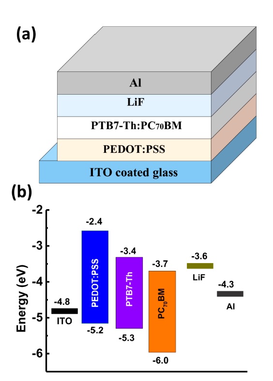
We used Lumerical, FDTD solution software, for performing 2-dimensional optical simulations of the PV device with the PTB7-Th):PC70BM active layer (Figure 1a). To define the optical properties of the different layers of the PV cell, we incorporated wavelength-dependent refractive indices and extinction coefficients (collected from previous reports) of different layers [18,19]. Next, the device structure was meshed at an optimum mesh density to minimize its effect on the simulation results.
Through optical simulations, the distribution of the electric field (photogenerated) owing to the absorption of photons within the photoactive layer was estimated. It was further used to calculate the ideal photogenerated short-circuit current density (Jsc,ideal) of the indoor OPV with the assumption of 100% internal quantum efficiency (IQE) [18]. Furthermore, we assumed that light travelled through the indoor OPV device at 90° to its surface (periodic boundaries along the x-axis were imposed). Finally, a continuous-wave normalized source was used to obtain the impulse response of the system. During the simulation (1000 lx LED light), the impulse response was multiplied with the respective source spectrum to obtain a user-defined power spectrum.
2.2 Device Fabrication
To fabricate the indoor OPV (Figure 1a), we first cleaned indium tin oxide (ITO)-coated (thickness: 150 nm) glass substrates (~10 Ω/sq) (All for LAB) using a detergent in a sonication bath. Then, we rinsed the substrates with deionized water, followed by acetone and isopropyl alcohol (Sigma-Aldrich) to remove all the detergent. Next, we dried the substrate by blowing nitrogen gas using a nitrogen gun. Subsequently, we spin-coated a hole transport layer (HTL) of poly(3,4-ethylenedioxythiophene):polystyrene sulfonate (PEDOT:PSS; Heraeus Epurio) (40 nm) onto the ITO layer at 3000 rpm for 60 s, and dried it through thermal annealing at 120 °C for 30 min on a hotplate in ambient air. We then transferred the HTL-coated substrate into a glove box and spin-coated a filtered solution (0.2 μm PTFE filter) of the active materials (PTB7-Th:PC70BM (1-Material) (1:1.5)) in chlorobenzene (Sigma-Aldrich) onto it at 800 rpm for 30 s, and dried it by annealing at 150 °C for 10 min in the glove box. The thickness of the active layer was fixed at ~100 nm (optimized through optical simulations). Next, we formed an ultrathin layer of lithium fluoride (LiF; thickness of ~0.5 nm) onto the active layer using a thermal evaporation technique at a pressure of <6 μPa and deposition rate of <0.1–0.2 nm/s. Finally, we deposited a ~100 nm thick cathode layer onto the LiF layer through the vacuum thermal deposition of Al at a pressure of <6 μPa and a deposition rate of <0.1–0.2 nm/s. The thermal evaporation was performed using a vacuum thermal evaporation system (Daedong High Tech Corporation). The active area of the device is 0.02 cm2.
3. RESULTS AND DISCUSSION
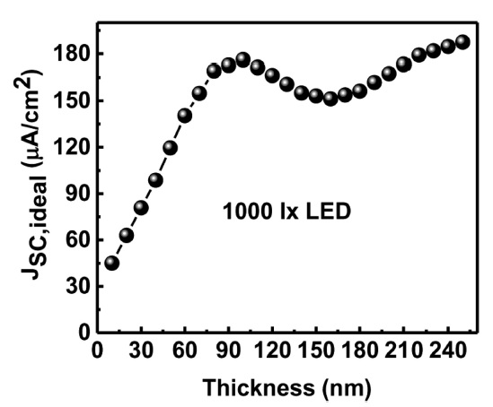
In this work, we considered PTB7-Th:PC70BM as the photoactive material of our indoor OPV device because it has good spectral matching with the irradiance spectra of the LED lamp [11,20]. Furthermore, the energy band alignment (Figure 1b) of the different layers of the OPV is optimal for developing a well-behaved OPV device for indoor application. Figure 1b shows that the highest occupied molecular orbital (HOMO) level of PTB7-Th is very close to the HOMO level of the PEDOT:PSS HTL. This is favorable for transporting holes towards the anode. Furthermore, the mismatch between the lowest unoccupied molecular orbital (LUMO) levels of the PTB7-Th and PEDOT:PSS layers blocks the movement of electrons towards the anode. However, a high optical band gap of PTB7-Th is favorable for developing an indoor OPV. Before fabricating the OPV device, we simulated the device performance through optical modeling for optimizing the thickness of its active layer. Figure 2 presents the variation in the simulated photogenerated Jsc,ideal of the OPV device with the thickness of the active layer under the illumination of 1000 lx LED light. Here, it can be noted that the simulated Jsc,ideal of the indoor OPV cell significantly depends on the thickness of the active layer; first, it gradually increases with increasing thickness of the active layer and then reaches a maximum value at 100 nm thickness, and subsequently decreases with a further increase in the active layer thickness up to a certain limit, and then increases again (i.e., it shows an oscillating nature) [21].

Variation in the simulated Jsc,ideal with the active layer thickness for an indoor OPV device (operated under the illumination of 1000 lx LED light).
Thicker active layers can absorb more photons than thinner ones, which is why the photogenerated Jsc,ideal of the device increased with the increase in the active layer thickness in the initial stage.
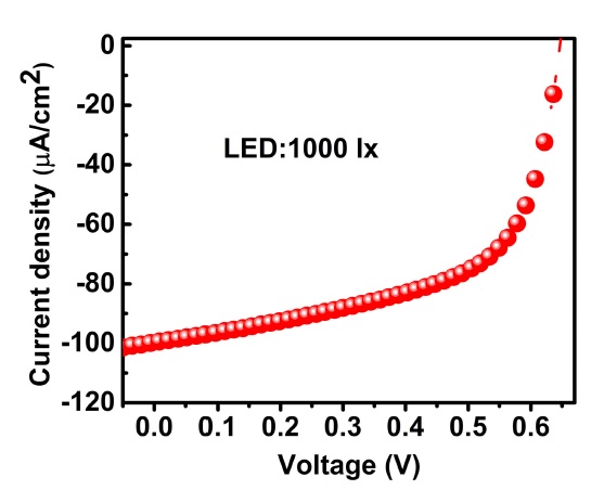
The oscillating nature of the Jsc,ideal with the active layer thickness may be attributed to the interference of the incident light and reflected light (from the back electrode) in the active layer of the device. For further investigation, we considered 100 nm as the optimized thickness of the indoor OPV because it corresponds to the first peak position of the active layer thickness-dependent Jsc,ideal. For a device with a thicker active layer, although the photogenerated Jsc,ideal would be very high, the actual short-circuit current density and thus the PCE value would be lower owing to the lower IQE value [18]. Next, we tested six OPVs fabricated with an active layer of optimized thickness (100 nm) under the illumination of a 1000 lx LED lamp (the LED light simulator was purchased from McScience, Republic of Korea). We recorded the voltage (V)-dependent current density (J) (measured using 2401, Keithley Instruments) of the device operated under the illumination of the LED lamp (Figure 3). The LED lamp used was a white linear COB LED from McScience. Various device performance parameters (average and maximum values) extracted from the J–V characteristics curve (under illuminating condition) are summarized in Table 1, which shows that the OPV with a 100 nm thick active layer exhibits a maximum JSC of 97.30 μA/cm2, PCE of 12.23%, and MPD of 44 μW/cm2 under the illumination of the 1000 lx LED lamp. The sufficiently high PCE and MPD values indicate that the device can be a good candidate as a powering aid for a low-power (μW range) sensor system. Furthermore from the standard deviated error values (Table 1) of different device performance parameters it can be observed that the variation is below 10%. This result implies that the physicochemical properties of different constituent materials of the device are uniformly distributed.

Variation in the current density (J) with the voltage (V) for an indoor OPV operating under the illumination of 1000 lx LED.
4. CONCLUSIONS
In this study, we fabricated a highly efficient indoor OPV with an ultrathin PTB7-Th:[PC70BM] active layer through the combination of optical simulation and experimental studies. The optical simulations suggested that the OPV can harvest the maximum amount of photon energy at 100 nm thickness of the active layer. In view of this result, we fabricated an OPV device with an active layer thickness of 100 nm. The device exhibited a maximum PCE of 12.23%, along with a short-circuit current density of 97.7 μA/cm2 and open circuit voltage of 0.66 V. It also exhibited an MPD of 44 μW/cm2, which is suitable for powering a low-power (μW range) sensor system.
Acknowledgments
This research was supported by the International Research & Development Program of the National Research Foundation of Korea (NRF) funded by the Ministry of Education, Science and Technology (MEST) of Korea (2019K1A3A1A21031246). This research was also supported by the Korea Institute of Industrial Technology under the “Development of Soft Robotics Technology for Human-Robot Coexistence Care Robots program (Grant Number: KITECH EH210010).
REFERENCES
-
R. A. Kjellby, L. R. Cenkeramaddi, T. E. Johnsrud, S. E. Løtveit, G. Jevne, B. Beferull-Lozano, and J. Soumya, “Self-powered IoT device based on energy harvesting for remote applications”, IEEE Int. Conf. Adv. Netw. Telecomm. Syst. (ANTS), IEEE, pp. 1-4, 2018.
[https://doi.org/10.1109/ANTS.2018.8710171]

-
F. Molaei, E. Rahimi, H. Siavoshi, S. G. Afrouz, and V. Tenorio, “A comprehensive review on internet of things (IoT) and its implications in the mining industry”, Am. J. Eng. Appl. Sci., Vol. 13, No. 3, pp. 499-515, 2020.
[https://doi.org/10.3844/ajeassp.2020.499.515]

-
M. Kassab, J. DeFranco, and P. Laplante, “A systematic literature review on Internet of things in education: Benefits and challenges”, J. Comput. Assist. Learn., Vol. 36, No. 2, pp. 115-127, 2020.
[https://doi.org/10.1111/jcal.12383]

-
S. Duangsuwan, A. Takarn, and P. Jamjareegulgarn, “A development on air pollution detection sensors based on NB-IoT network for smart cities”, 18th Int. Symp. on Commun. Inf. Technol. (ISCIT), IEEE, pp. 313-317, 2018.
[https://doi.org/10.1109/ISCIT.2018.8587978]

-
S. K. Roy, S. Misra, and N. S. Raghuwanshi, “Sens, PnP: Seamless integration of heterogeneous sensors with IoT devices”, IEEE Trans. Consum. Electron., Vol. 65, No. 2, pp. 205-214, 2019.
[https://doi.org/10.1109/TCE.2019.2903351]

-
A. Kaliwo and C. Mikeka, “Tackling the issues of powering mobile IoT sensors and systems using off-grid sources of energy, the case of the real-time web-based temperature monitoring system in Malawi”, Int. Conf. e-Infrastruct. e-Serv. Dev. Ctries, Springer, pp. 232-238, 2018.
[https://doi.org/10.1007/978-3-319-98827-6_21]

-
A. Bakytbekov, T. Q. Nguyen, W. Li, A. L. Lee Cottrill, G. Zhang, M. S. Strano, K. N. Salama, and A. Shamim, “Multi-source ambient energy harvester based on RF and thermal energy: Design, testing, and IoT application”, Energy Sci. Eng., Vol. 8, No. 11, pp. 3883-3897, 2020.
[https://doi.org/10.1002/ese3.784]

-
O. A. Saraereh, A. Alsaraira, I. Khan, and B. J. Choi, “A hybrid energy harvesting design for on-body internet-of-things (IoT) networks”, Sensors (Basel), Vol. 20, No. 2, pp. 407(1)-407(16), 2020.
[https://doi.org/10.3390/s20020407]

-
C. Jiang, X. Li, S. W. M. Lian, Y. Ying, J. S. Ho, and J. Ping, “Wireless technologies for energy harvesting and transmission for ambient self-powered systems”, ACS Nano, Vol. 15, No. 6, pp. 9328-9354, 2021.
[https://doi.org/10.1021/acsnano.1c02819]

-
A. S. Adila, A. Husam, and G. Husi, “Towards the self-powered Internet of things (IoT) by energy harvesting: Trends and technologies for green IoT”, 2nd Int. Symp. Small-scale Intell. Manuf. Syst. (SIMS), IEEE, pp. 1-5, 2018.
[https://doi.org/10.1109/SIMS.2018.8355305]

-
S. Biswas and H. Kim, “Solar cells for indoor applications: Progress and development”, Polymers, Vol. 12, No. 6, pp. 1338(1)-1338(23), 2020.
[https://doi.org/10.3390/polym12061338]

-
Y. Cui, L. Hong, and J. Hou, “Organic photovoltaic cells for indoor applications: Opportunities and challenges”, ACS Appl. Mater. Interfaces, Vol. 12, No. 35, pp. 38815-38828, 2020.
[https://doi.org/10.1021/acsami.0c10444]

-
B. Zimmermann, and U. Würfel, “Organic photovoltaic cells and modules for applications under indoor lighting conditions,” Indoor Photovoltaics: Materials, Modeling and Applications, Wiley, pp. 189-211, 2020.
[https://doi.org/10.1002/9781119605768.ch7]

-
S. Biswas, Y. J. You, J. W. Shim, and H. Kim, “Utilization of poly (4-styrenesulfonic acid) doped polyaniline as a hole transport layer of organic solar cell for indoor applications”, Thin Solid Films, Vol. 700, p. 137921, 2020.
[https://doi.org/10.1016/j.tsf.2020.137921]

-
S. Biswas, Y. J. You, Y. Lee, J. W. Shim, and H. Kim, “Efficiency improvement of indoor organic solar cell by optimization of the doping level of the hole extraction layer”, Dyes Pigm., Vol. 183, p. 108719, 2020.
[https://doi.org/10.1016/j.dyepig.2020.108719]

-
S. Biswas, Y. J. You, P. Vincent, J. H. Bae, J. W. Shim, and H. Kim, “Organic tandem solar cells under indoor light illumination”, Prog. Photovolt. Res. Appl., Vol. 28, No. 9, pp. 946-955, 2020.
[https://doi.org/10.1002/pip.3301]

- S. Biswas and H. Kim, “Optical simulation study on indoor organic photovoltaics with textured electrodes towards self-powered photodetector”, J. Sens. Sci. Technol., Vol. 28, No. 4, pp. 236-239, 2019.
-
P. Vincent, S. C. Shin, J. S. Goo, Y. J. You, B. Cho, S. Lee, D. W. Lee, S. R. Kwon, K. B. Chung, and J. J. Lee, J. Bae, J. W. Shim, and H. Kim, “Indoor-type photovoltaics with organic solar cells through optimal design”, Dyes Pigm., Vol. 159, pp. 306-313, 2018.
[https://doi.org/10.1016/j.dyepig.2018.06.025]

-
J. Mescher, A. Mertens, A. Egel, S. W. Kettlitz, U. Lemmer, and A. Colsmann, “Illumination angle and layer thickness influence on the photo current generation in organic solar cells: A combined simulative and experimental study”, AIP Adv., Vol. 5, No. 7, p. 077188, 2015.
[https://doi.org/10.1063/1.4928074]

-
W. Xu, C. Yi, X. Yao, L. Jiang, X. Gong, and Y. Cao, “Efficient organic solar cells with polymer-small molecule: Fullerene ternary active layers”, ACS Omega, Vol. 2, No. 5, pp. 1786-1794, 2017.
[https://doi.org/10.1021/acsomega.7b00269]

-
J. Gilot, I. Barbu, M. M. Wienk, and R. A. J. Janssen, “The use of ZnO as optical spacer in polymer solar cells: Theoretical and experimental study”, Appl. Phys. Lett., Vol. 91, No. 11, p. 113520, 2007.
[https://doi.org/10.1063/1.2784961]


