Photocurrent Characteristics of Gate/Body-Tied MOSFET-Type Photodetector with High Sensitivity
This is an Open Access article distributed under the terms of the Creative Commons Attribution Non-Commercial License(https://creativecommons.org/licenses/by-nc/3.0/) which permits unrestricted non-commercial use, distribution, and reproduction in any medium, provided the original work is properly cited.
Abstract
In this paper, the photocurrent characteristics of gate/body-tied (GBT) metal-oxide semiconductor field-effect transistor (MOSFET)-type photodetector with high sensitivity in the 408 nm – 941 nm range are presented. High sensitivity is important for photodetectors, which are used in several scientific and industrial applications. Owing to its inherent amplifying characteristics, the GBT MOSFET-type photodetector exhibits high sensitivity. The presented GBT MOSFET-type photodetector was designed and fabricated via a standard 0.18 μm complementary metal-oxide-semiconductor (CMOS) process, and its characteristics were analyzed. The photodetector was analyzed with respect to its width to length (W/L) ratio, bias voltage, and incident-light wavelength. It was confirmed experimentally that the presented GBT MOSFET-type photodetector has over 100 times higher sensitivity than a PN-junction photodiode with the same area in the 408 nm – 941 nm range.
Keywords:
Gate/body-tied, Photodetector, MOSFET, Sensitivity, PN-junction photodiode, Wavelength1. INTRODUCTION
As a tool for acquiring image information, a highly integrated and high-efficiency complementary metal-oxide-semiconductor (CMOS) image sensor can use various peripheral circuits for additional functions and has the advantage of low cost. Consequently, they are being used in various fields, and related research is being actively conducted [1-3]. Recently, among the main research fields of CMOS image sensors, photodetectors with high sensitivity have been actively studied with regard to their scientific and industrial applications, such as in light detection and ranging (LiDAR), time-of-flight (ToF), 3D imaging and fluorescence lifetime-imaging-microscopy systems [4-7].
Single photon avalanche photodiodes (SPADs), which operate in an avalanche mode above the breakdown level, have been used for similar purposes. SPADs can be fabricated using the CMOS technology, however, they have the disadvantage of possessing a large pixel area and requiring a high supply voltage. Moreover, to manufacture a high-resolution image sensor based on SPADs, quenching circuits and time-to-digital converter circuits are essential, making the signal processing complicated [8-11].
In this paper, a gate/body-tied (GBT) metal-oxide semiconductor field-effect transistor (MOSFET)-type photodetector possessing a small pixel area and requiring a low supply voltage with high sensitivity in the 408 nm – 941 nm range is presented. Previously, it was confirmed that the GBT MOSFET-type photodetector exhibits high sensitivity to blue (473 nm), green (533 nm) and red (633 nm) light, owing to its inherent amplifying characteristics [12]. In this study, a GBT MOSFET-type photodetector was designed and fabricated via a standard 0.18 μm CMOS process. In the analysis, the photocurrent characteristics of the GBT MOSFET-type photodetector with respect to source voltage, width to length (W/L) ratio, and incident-light wavelength were measured. In addition, the photocurrent characteristics were compared with those of a PN-junction photodiode with the same area in the 408 nm-941 nm range.
2. PRINCIPLE OF OPERATION
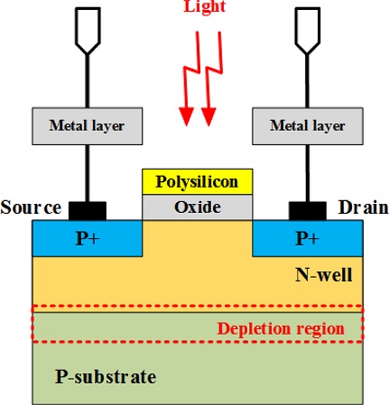
Fig. 1 shows the vertical structure of a GBT MOSFET-type photodetector. The photodetector is designed such that the gate node and the body node are physically connected. The area of the photodetector, excluding the gate, is shielded by a metal wire. The gate consists of polysilicon. As a result, light strikes only the gate region of the photodetector. Some photons of short wavelengths are absorbed in the polysilicon gate, resulting in the reduction of sensitivity, whereas photons with long wavelengths are mostly absorbed by the substrate. The incident light entering through the gate of the photodetector generates electron-hole pairs in the depletion region. The holes drift toward the channel and P substrate, and the electrons accumulate in the N-well owing to the high potential barrier. These accumulated electrons reduce the potential barrier of the N-well, which cause a negative gate voltage of photodetector, because the gate is connected to the N-well. Because of decrease in the gate voltage, a channel is formed and current flows through the channel. In addition, the accumulated electrons generate a negative voltage in the N-well, and a positive feedback to the gate through the gate/N-well connection is created. The photocurrent of the GBT MOSFET-type photodetector is highly amplified by this positive feedback mechanism [13-15].
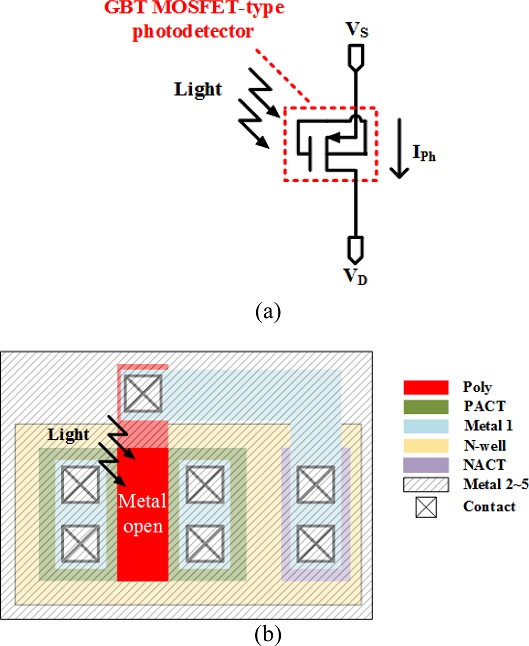
Fig. 2 (a) shows the symbol of a single GBT MOSFET-type photodetector for measuring the photocurrent. To measure the photocurrent (Iph) generated by the light incident on the active region of the photodetector, the GBT MOSFET-type photodetector was designed with the structure presented in Fig. 1(a). Fig. 1 (b) shows the layout of the photodetector. The gate node of the photodetector depicted in Fig. 2 was designed to be physically tied with the body node.
3. EXPERIMENTAL RESULTS AND DISCUSSIONS
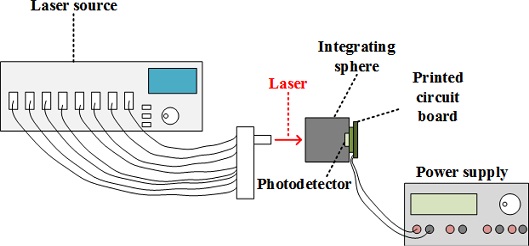
Fig. 3 shows the experimental environment for photocurrent measurement of photodetectors. Using a laser source, the incident light was emitted with a total of 8 wavelengths: 408 nm, 489 nm, 521 nm, 639 nm, 726 nm, 785 nm, 854 nm, and 941 nm. In the setup, the light from the laser source enters the integrating sphere, inside which repeated Lambertian reflections occur. The reflected light has a uniform distribution and is incident on the photodetector. The photodetector was fabricated using the standard 0.18 μm CMOS process. Threshold voltage of the fabricated p-channel MOSFET operating in the enhancement mode was -0.4 V.
The GBT MOSFET-type photodetector is essentially a MOSFET. The voltage between the source and drain nodes (VSD) determines the operating region of the photodetector. In this region, a photocurrent is generated by the light incident at the photodetector. Therefore, to use the GBT MOSFET-type photodetector as a photodetector, it is essential to analyze its characteristics with respect to VSD. In addition, a general characteristic of a MOSFET-type photodetector is that the output signal is affected by the W/L ratio of the device. Therefore, it is essential to analyze the photocurrent characteristics of the GBT MOSFET-type photodetector with respect to the W/L ratio.
Fig. 4 shows photocurrent-measurement results with respect to the source voltage of the photodetector for various wavelengths. As a light source, output light wavelengths of 408 nm, 785 nm, and 941 nm of the laser source were used. The optical power of the three wavelengths was measured as 100 μW under the same conditions as above. It can be observed in Fig.4 that among the three wavelengths tested, 785 nm generated the greatest photocurrent in the photodetector. Therefore, it can be inferred that the sensitivity is the highest when the wavelength of the light incident on the GBT MOSFET-type photodetector is 785 nm.
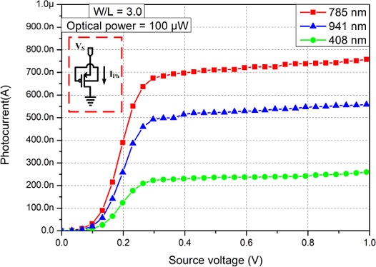
Photocurrent-measurement results with respect to the source voltage of GBT MOSFET-type photodetector for various wavelengths.
Table 1 shows various widths and lengths and the corresponding W/L ratios of the GBT MOSFET-type photodetector with the same area (4 μm2). Fig. 5 shows the photocurrent-measurement results with respect to the source voltage of the photodetector for various W/L ratios. It can be observed that as the W/L ratio of the photodetector increased from 0.3 to 3.0, the generated photocurrent increased from approximately 148 nA to 757 nA. Therefore, the sensitivity of the GBT MOSFET-type photodetector can be increased by adjusting its W/L.

Various widths and lengths and the corresponding W/L ratios of GBT MOSFET-type photodetector with the same area (4 μm2).
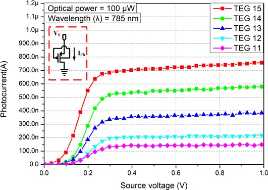
Photocurrent-measurement results with respect to the source voltage of GBT MOSFET-type photodetector for various W/L ratios.
Fig. 6 shows (a) the photocurrent-measurement results of the GBT MOSFET-type photodetector with respect to the wavelength of the incident light and (b) the photocurrent-measurement results of a PN-junction photodiode with respect to the wavelength of the incident light. Table 2 lists: (a) the photocurrent measurements of the GBT MOSFET-type photodetector (IGBT) and that of the PN-junction photodiode (IPN) with the same area, and (b) the corresponding wavelengths of the incident light.
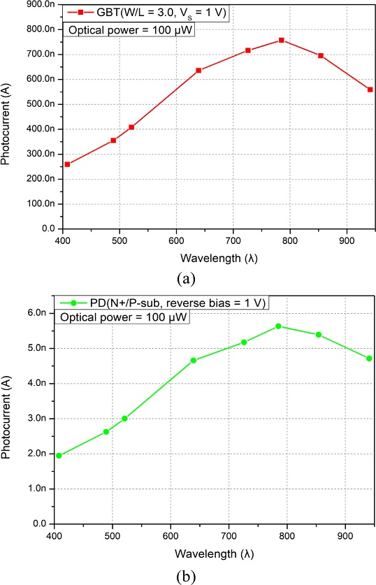
(a) Photocurrent-measurement results of the GBT MOSFET-type photodetector with respect to incident-light wavelength and (b) photocurrent-measurement results of a PN-junction photodiode with respect to incident-light wavelength.

Photocurrent of the GBT MOSFET-type photodetector (IGBT) and that of the PN-junction photodiode (IPN) with the same area with respect to incident-light wavelength.
To measure the photocurrent, the source voltage of the GBT MOSFET-type photodetector and PN-junction photodiode of the same area were measured at 1 V and reverse bias 1 V, respectively. In the case of the PN-junction photodiode, the measured photocurrent at the full wavelength ranged from approximately 1.95 nA to 5.63 nA, and that for the GBT MOSFET-type photodetector, the photocurrent is about 259 nA to 757 nA. On comparing these two photocurrent measurements, it was confirmed that the optical properties of the GBT MOSFET-type photodetector were excellent at a wavelength of 408 nm – 941 nm.
4. CONCLUSIONS
In this study, a GBT MOSFET-type photodetector was designed and fabricated via a standard 0.18 μm CMOS process. The characteristics of the photocurrent with respect to the source voltage, width to length (W/L) ratio of the photodetector, and wavelength of the incident light were evaluated through measurements. In addition, the photocurrent characteristics of the photodetector with high sensitivity at a wavelength of 408 nm – 941 nm was measured and compared with those of a PN-junction photodiode.
It is known that the responsivity of a Si PN-junction photodiode is typically 0.3 A/W to 0.5 A/W. Because, in this study, the photocurrent of the GBT MOSFET-type photodetector was found to be over 100 times greater than that of the PN-junction photodiode with the same area, the responsivity of the photodetector is estimated to be over 30 A/W. Therefore, the presented photodetector can be useful for several applications; particularly, those requiring high sensitivity in the visible and near infrared (NIR) range.
Acknowledgments
This research was supported by Samsung Electronics Company, Basic Science Research Program through the National Research Foundation of Korea (NRF) funded by the Ministry of Education (2018R1D1A3B0704995213), and the Integrated Circuit Design Education Center (IDEC) in Korea, and we are grateful for this. We also thank the photometry and radiometry group of Korea Research Institute of Standards and Science (KRISS) for supporting the photocurrent measurement.
REFERENCES
-
L. Yao, K. Y. Yung, R. Khan, V. P. Chodavarapu, and F. V. Bright, “CMOS Imaging of Pin-Printed Xerogel-Based Luminescent Sensor Microarrays”, IEEE Sens. J., Vol. 10, No. 12, pp. 1824-1832, 2010.
[https://doi.org/10.1109/JSEN.2010.2047497]

-
E. R. Fossum, “CMOS image sensors: electronic camera-on-a-chip”, IEEE Trans. Electron Devices, Vol. 44, No. 10, pp. 1689-1698, 1997.
[https://doi.org/10.1109/16.628824]

-
M. Bigas, E. Cabruja, J. Forest, and J. Salvi, “Review of CMOS image sensors”, Microelectronics J., Vol. 37, No. 5, pp. 433-451, 2006.
[https://doi.org/10.1016/j.mejo.2005.07.002]

-
A. Dieguez, O. Alonso, E. Vilella, and A. Vila, “A Verilog-A model for the design of devices for fluorescence life-time measurement with CMOS SPADs”, 2015 Int. Conf. Synth. Model. Anal. Simul. Methods Appl. to Circuit Des. SMACD 2015, pp. 1-4, 2015.
[https://doi.org/10.1109/SMACD.2015.7301680]

-
S. Lindner, C. Zhang, I. M. Antolovic, M. Wolf, and E. Charbon, “A 252 × 144 SPAD Pixel Flash Lidar with 1728 Dual-Clock 48.8 PS TDCs, Integrated Histogramming and 14.9-to-1 Compression in 180NM CMOS Technology”, IEEE Symp. VLSI Circuits, Dig. Tech. Pap., pp. 69-70, 2018.
[https://doi.org/10.1109/VLSIC.2018.8502386]

-
W. Shi and A. Pan, “Mixed Design of SPAD Array Based TOF for Depth Camera and Unmanned Vehicle Applications”, SMACD 2018 - 15th Int. Conf. Synth. Model. Anal. Simul. Methods Appl. to Circuit Des., pp. 277-280, 2018.
[https://doi.org/10.1109/SMACD.2018.8434860]

-
J. Kekkonen, T. Talala, J. Nissinen, and I. Nissinen, “On the Spectral Quality of Time-Resolved CMOS SPAD-Based Raman Spectroscopy with High Fluorescence Backgrounds”, IEEE Sens. J., Vol. 20, No. 9, pp. 4635-4645, 2020.
[https://doi.org/10.1109/JSEN.2020.2966119]

-
L. Frey, M. Marty, S. Andre, and N. Moussy, “Enhancing Near-Infrared Photodetection Efficiency in SPAD with Silicon Surface Nanostructuration”, IEEE J. Electron Devices Soc., Vol. 6, No. 1, pp. 392-395, 2018.
[https://doi.org/10.1109/JEDS.2018.2810509]

-
J. M. Pavia, M. Scandini, S. Lindner, M. Wolf, and E. Charbon, “A 1 × 400 Backside-Illuminated SPAD Sensor with 49.7 ps Resolution, 30 pJ/Sample TDCs Fabricated in 3D CMOS Technology for Near-Infrared Optical Tomography”, IEEE J. Solid-State Circuits, Vol. 50, No. 10, pp. 2406-2418, 2015.
[https://doi.org/10.1109/JSSC.2015.2467170]

-
I. Vornicu, R. Carmona-Galan, and A. Rodriguez-Vazquez, “On the calibration of a SPAD-based 3D imager with in-pixel TDC using a time-gated technique”, Proc. IEEE Int. Symp. Circuits Syst., pp. 1102-1105, 2015.
[https://doi.org/10.1109/ISCAS.2015.7168830]

-
C. Zhang, S. Lindner, I. M. Antolovic, J. Mata Pavia, M. Wolf, and E. Charbon, “A 30-frames/s, 252 × 144 SPAD Flash LiDAR with 1728 Dual-Clock 48.8-ps TDCs, and Pixel-Wise Integrated Histogramming”, IEEE J. Solid-State Circuits, Vol. 54, No. 4, pp. 1137-1151, 2019.
[https://doi.org/10.1109/JSSC.2018.2883720]

- S. H. Seo, K. Do Kim, M. W. Seo, J. S. Kong, J. K. Shin, and P. Choi, “Optical characteristics of an N-Well/gate-tied PMOSFET-type photodetector with built-in transfer gate for CMOS image sensor”, Sensors Mater., Vol. 19, No. 7, pp. 435-444, 2007.
-
H. Kwen, S. H. Kim, J. Lee, P. Choi, and J. K. Shin, “Simulation of High-Speed and Low-Power CMOS Binary Image Sensor Based on Gate/Body-Tied PMOSFET-Type Photodetector Using Double-Tail Comparator”, J. Sens. Sci. Technol., Vol. 29, No. 2, pp. 82-88, 2020.
[https://doi.org/10.5369/JSST.2020.29.2.82]

-
S. H. Kim, H. Kwen, J. Jang, Y. M. Kim, and J. K. Shin, “2500 fps High-Speed Binary CMOS Image Sensor Using Gate/Body-Tied Type High-Sensitivity Photodetector”, J. Sens. Sci. Technol., Vol. 30, No. 1, pp. 61-65, 2021.
[https://doi.org/10.46670/JSST.2021.30.1.61]

-
J. Jang, J. Lee, H. Kwen, S. H. Seo, P. Choi, and J. K. Shin, “Adjusting the Sensitivity of an Active Pixel Sensor Using a Gate/Body-Tied P-Channel Metal-Oxide Semiconductor Field-Effect Transistor-Type Photodetector With a Transfer Gate”, J. Sens. Sci. Technol., Vol. 30, No. 2, pp. 114-118, 2021.
[https://doi.org/10.46670/JSST.2021.30.2.114]

