Floating Inverter Amplifiers with Enhanced Voltage Gains Employing Cross-Coupled Body Biasing
This is an Open Access article distributed under the terms of the Creative Commons Attribution Non-Commercial License(https://creativecommons.org/licenses/by-nc/3.0/) which permits unrestricted non-commercial use, distribution, and reproduction in any medium, provided the original work is properly cited.
Abstract
Floating inverter amplifiers (FIAs) have recently garnered considerable attention owing to their high energy efficiency and inherent resilience to input common-mode voltages and process-voltage-temperature variations. Since the voltage gain of a simple FIA is low, it is typically cascaded or cascoded to achieve a higher voltage gain. However, cascading poses stability concerns in closed-loop applications, while cascoding limits the output swing. This study introduces a gain-enhanced FIA that features cross-coupled body biasing. Through simulations, it is demonstrated that the proposed FIA designed using a 28-nm complementary metal-oxide-semiconductor technology with a 1-V power supply can achieve a high voltage gain (> 90 dB) suitable for dynamic open-loop applications. The proposed FIA can also be used as a closed-loop amplifier by adjusting the amount of positive feedback due to the cross-coupled body biasing. The capability of achieving a high gain with minimum-length devices makes the proposed FIA a promising candidate for low-power, high-speed sensor interface systems.
Keywords:
Dynamic amplifier, Floating inverter amplifier, Body biasing1. INTRODUCTION
Amplifiers are one of the most important building blocks in the analog sensor interface circuitry. A high voltage gain is desirable for precision operation; however, achieving a high gain is becoming increasingly challenging in advanced semiconductor technologies with a low supply voltage. Furthermore, conventional amplifiers suffer from low energy efficiency owing to their static current consumption.
In modern technologies optimized for digital circuitry, complimentary metal-oxide-semiconductor (CMOS) inverters are considered to be energy-efficient analog amplifiers [1,2]. The CMOS inverter uses the transconductance of both the NMOS and PMOS transistors, utilizing the same bias current. As a result, a higher bandwidth is available for the same current consumption. Consequently, CMOS inverters have been used in various analog applications [2].
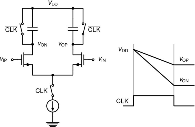
As an alternative to conventional amplifiers, dynamic amplifiers have been introduced to improve the energy efficiency [3-6]. Instead of using a constant bias current, a dynamic amplifier uses only the required current to charge the output capacitance and develop the output voltage, as illustrated in Fig. 1. The gain of the dynamic amplifier depends on the amplification duration, which is limited by the common-mode current. Given the supply voltage, the voltage gain can be increased by reducing the common-mode current; however, the operating speed will be lowered. Another difficulty with the dynamic amplifier shown in Fig. 1 is that the output common-mode voltage is not constant.
Recently, floating inverter amplifiers (FIAs) have emerged as dynamic amplifiers that employ CMOS inverters [7,8]. A salient feature of the FIA is that its common-mode output voltage remains almost constant over a broad range of input common-mode voltages. Additionally, an FIA features a self-quenching mechanism that reduces energy consumption. While initially intended as a pre-amplifier for a comparator, FIAs are now extensively employed in the implementation of closed-loop amplifiers for energy-efficient analog-to-digital converters (ADCs) [9-15].
This paper briefly reviews the operation of an FIA and presents a technique for enhancing the voltage gain of a simple FIA without compromising the signal swing or increasing the circuit size.
2. FLOATING INVERTER AMPLIFIER
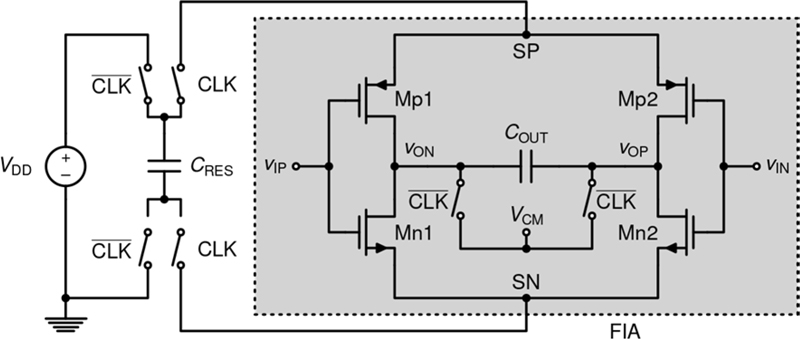
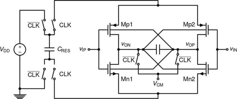
A basic FIA is illustrated in Fig. 2. Instead of a fixed power supply, the CMOS inverters are powered by a reservoir capacitor (CRES). Prior to amplification, the reservoir capacitor is charged to VDD, and the output capacitors are reset to the desired output common-mode voltage (VCM). During the amplification phase, the stored charges in the reservoir capacitor are utilized to develop the differential output. If the reservoir capacitor is sufficiently small, the voltages at nodes SP and SN approach each other, and eventually all the transistors are almost turned off. Since only the small lost charges need to be replenished during the reset cycle, the FIA exhibits high energy efficiency.
A crucial characteristic of the FIA is that the current exiting the positive terminal of the reservoir capacitor must return to the negative terminal. Consequently, the output common-mode voltage cannot change provided that the parasitic capacitances at nodes SP and SN are negligible. Since the output common-mode voltage is well controlled without an additional common-mode feedback circuit, the FIA facilitates straightforward interfacing with other circuits.
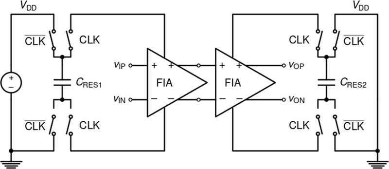
When the reservoir capacitor is extremely large, the FIA is similar to a conventional inverter amplifier. Consequently, the voltage gain of the FIA is limited to that of a CMOS inverter, which is approximately 10 for minimum-length devices in a 28-nm CMOS technology. The FIA can be cascaded to increase the overall gain, as shown in Fig. 3 [9-11,15]. However, cascading of FIAs introduces additional poles, thereby posing stability concerns when used in a closed-loop amplifier configuration. Appropriate sizing of the reservoir capacitors in cascaded FIAs can maintain a reasonable phase margin [10,11], but the use of multiple reservoir capacitors increases the circuit size and power consumption.
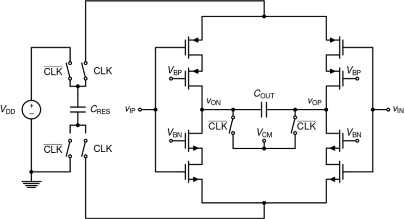
Alternatively, a cascoded FIA can be used to increase the gain, as shown in Fig. 4 [10,11,14,15]. The cascoded FIA requires a bias generation circuit that consumes a static current. For simplicity, the mid-voltage (the desired output commonmode voltage) can be used to bias the cascode devices, but the gain is prone to process-voltage-temperature (PVT) variations [15]. The cascode devices can be biased by the input signals, but it requires specialized low-threshold and high-threshold devices [10]. Another drawback of the cascoded FIA is that the output signal swing is reduced. Therefore, the voltage gain of the FIA needs to be enhanced without compromising the signal swing or increasing the circuit size, as detailed in the following section.
3. FLOATING INVERTER AMPLIFIER WITH BODY BIASING
3.1 Floating Inverter Amplifier with Body Biasing as Open-loop Dynamic Amplifier
During the amplification mode of the FIA in Fig. 2, the charges in the reservoir capacitor are transferred to the output capacitor. If the charges move through the pairs (Mp1 and Mn2) or (Mp2 and Mn1), an output differential signal develops. Conversely, if the charges traverse through the pairs (Mp1 and Mn1) or (Mp2 and Mn2), they have no effect on the output differential signal.
To maximize the output differential signal and thereby enhance the gain of the FIA, it is crucial to minimize the unnecessary current through the pairs (Mp1 and Mn1) or (Mp2 and Mn2). For example, when the input differential signal is positive, the current through Mp1 or Mn2 should be suppressed. This can be achieved by increasing the threshold voltages for Mp1 and Mn2. As illustrated in Fig. 5, tying the body terminals of Mp1 and Mn2 to the positive and negative output terminals, respectively, increases their threshold voltages. Meanwhile, the threshold voltages of Mn1 and Mp2 decrease, boosting the differential output current. This is a positive-feedback system that drives the output in a certain direction based on the polarity of the input signal. As a dynamic amplifier, the magnitude of the output signal depends on both the input magnitude and the duration of amplification.
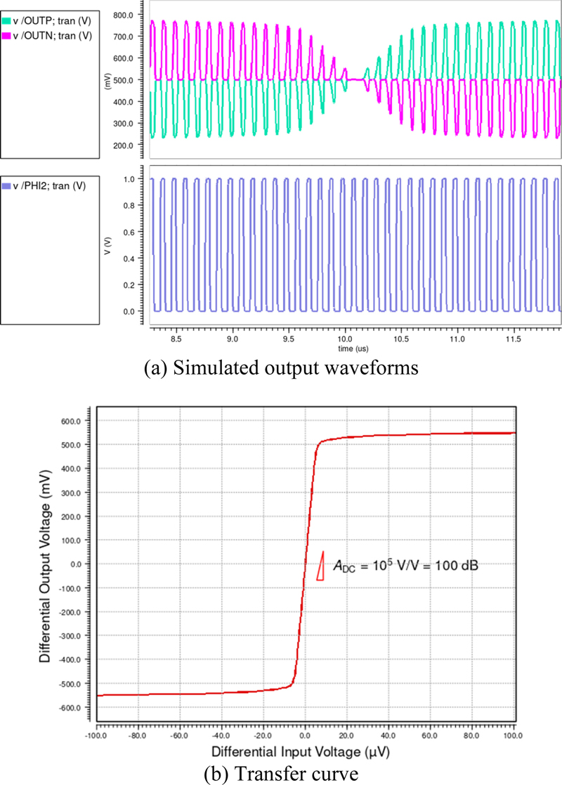
Fig. 6(a) illustrates the simulated output waveforms of the proposed FIA for the ramp input signal. Each transistor is identical in size, with a channel width and length of 6 mm and 30 nm, respectively. The supply voltage is 1 V, and the clock period is 100 ns. The reservoir capacitance is 2 pF, and the output capacitance is 250 fF. Fig. 6(b) shows the transfer curve of the proposed FIA, revealing a notable gain as high as 100 dB.
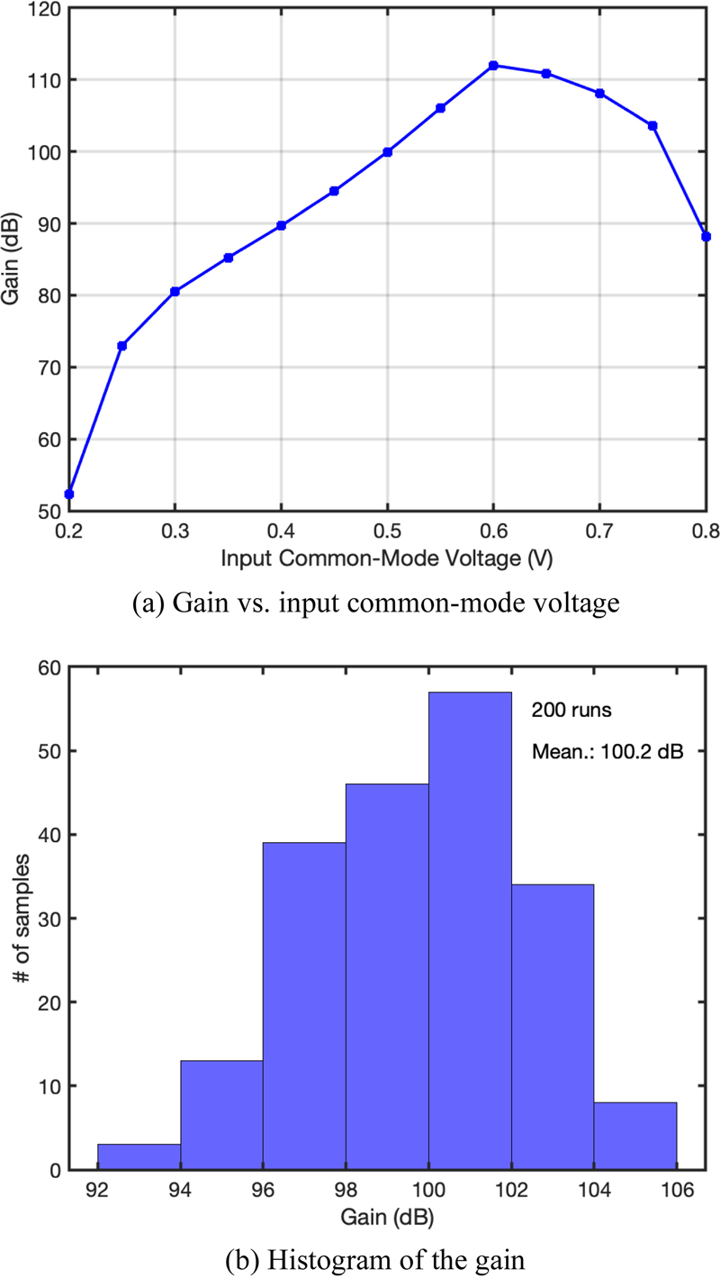
The gain of the proposed FIA is influenced by both the input common-mode voltage and PVT variations. Fig. 7(a) shows the gain as a function of the input common-mode voltage. Despite the impact of input common-mode voltages, the FIA maintains a high gain (>80 dB) within the range of input common-mode voltages from 0.3 V to 0.8 V. Fig. 7(b) presents the Monte-Carlo simulation results over process variations, demonstrating that the gain remains well above 90 dB.
3.2 Floating Inverter Amplifier with Body Biasing as Closed-loop Amplifier
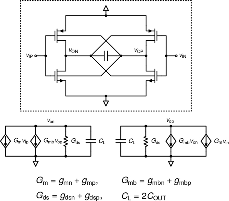
The FIA proposed in the previous subsection is based on a positive feedback system. An analysis using the small-signal model depicted in Fig. 8 reveals that the transfer function is expressed as
| (1) |
In the typical case where Gmb > Gds, the transfer function exhibits a right-half-plane pole. This characteristic renders the FIA with body biasing unstable, thereby preventing its application in closed-loop configurations. Once the charging direction of the output capacitor is set by the initial input polarity, subsequent control using the feedback signal becomes unfeasible.
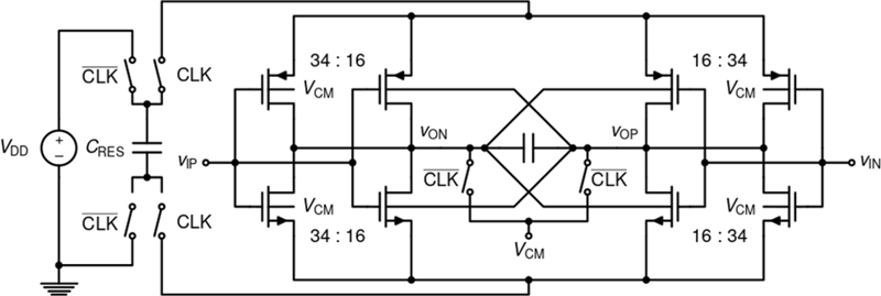
To address this problem, the transistors that constitute the floating inverters can be divided, and body biasing can be selectively applied, as shown in Fig. 9. By adopting this approach, the effective transconductance due to the body terminal can be reduced, relocating the right-half-plane pole to the left-half plane. While reducing the effective gain of the FIA, it unlocks the potential for utilizing the FIA with body biasing as a closed-loop amplifier.
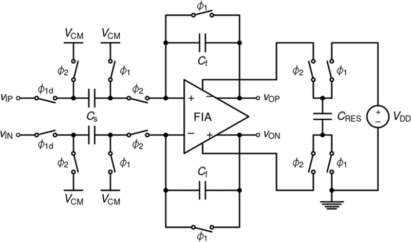
Fig. 10 shows a switched-capacitor (SC) amplifier that incorporates the proposed FIA. The gain of an SC amplifier is ideally determined by the capacitor ratio when the gain of the operational transconductance amplifier (OTA) is infinite. However, if the OTA has a finite gain (Adc), the gain of the SC amplifier is given by
| (2) |
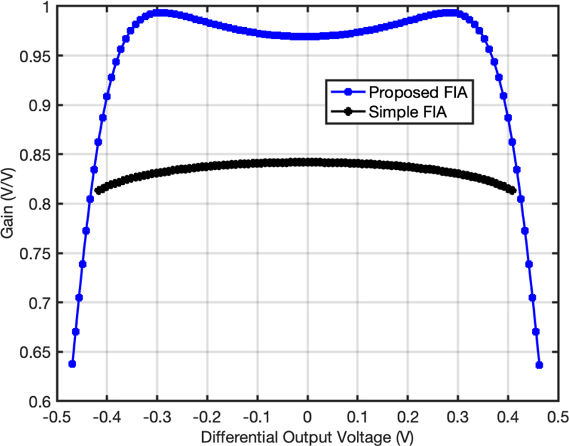
Fig. 11 shows the gains of the SC amplifiers as functions of the output voltage. In these simulations, both sampling (Cs) and feedback (Cf) capacitors have equivalent capacitances of 500 fF. Compared with the case of a simple FIA that has a voltage gain of approximately 10, the SC amplifier that employs the proposed FIA exhibits gains much closer to the ideal value of unity. The simulated gain of the SC amplifier using the proposed FIA is approximately 0.969, indicating an estimated gain of 62.5 for the proposed FIA. It should be noted that the voltage gain is achieved using minimum-length devices and that the voltage swing is comparable to that of a simple FIA. A higher gain can be achieved using devices with longer channel lengths.
Unfortunately, the proposed FIA is expected to be susceptible to device mismatches. Therefore, it is essential to carefully select the size ratio of the transistors with fixed and cross-coupled body biasing to maximize the gain while avoiding the instability caused by positive feedback. Calibration may be required to mitigate the impact of mismatch.
The proposed FIA could be also used to implement an SC integrator. SC integrators have extensive applications in noise-shaping ADCs. Since the DC gain of the OTA influences the in-band quantization noise floor, the increased gain provided by the proposed FIA is useful for achieving a sharper noise transfer function, particularly in low-power applications.
4. CONCLUSIONS
The FIA is a promising amplifier structure for advanced process nodes. Its output common-mode voltage is well-defined across a wide range of input common-mode voltages, and its low-power operation is particularly beneficial for sensor interfaces. However, the inherent limitation lies in the typically low voltage gain. It is necessary to cascade several simple FIAs, or use a cascode structure. Cascading introduces additional poles, posing a threat to the stability of closed-loop amplifiers, and the cascode FIA suffers from a limited output swing.
Through simulations, this study demonstrated that the voltage gain of an FIA can be enhanced by employing cross-coupled body biasing. In an open-loop amplifier configuration, aggressive cross-coupled body biasing can yield a voltage gain that exceeds 90 dB. In a closed-loop amplifier configuration, a more restrained application of body biasing is required to maintain stability. The advantage of achieving a high gain with short-channel devices suggests that the proposed FIA can be deployed in high-speed low-power sensor systems.
Acknowledgments
The EDA tools were supported by the IC Design Education Center (IDEC).
REFERENCES
-
Y. Chae and G. Han, “Low voltage, low power, inverter-based switched-capacitor Delta-Sigma modulator”, IEEE J. Solid-State Circuits, Vol. 44, No. 2, pp. 458-472, 2009.
[https://doi.org/10.1109/JSSC.2008.2010973]

-
W. Bae, “CMOS inverter as analog circuit: An overview”, J. Low Power Electron. Appl., Vol. 9, No. 3, pp. 26(1)-26(15), 2019.
[https://doi.org/10.3390/jlpea9030026]

-
J. Lin, M. Miyahara, and A. Matsuzawa, “A 15.5 dB, wide signal swing, dynamic amplifier using a common-mode voltage detection technique”, Proc. of 2011 IEEE Int. Symp. Circuits. Syst. (ISCAS), pp. 21-24, Rio de Janeiro, Brazil, 2011.
[https://doi.org/10.1109/ISCAS.2011.5937491]

-
F. V. D. Goes, C. M. Ward, S. Astgimath, H. Yan, J. Riley, Z. Zeng, J. Mulder, S. Wang, and K. Bult, “A 1.5 mW 68 dB SNDR 80 MS/s 2x interleaved pipelined SAR ADC in 28 nm CMOS”, IEEE J. Solid-Sstate Circuits, Vol. 49, No. 12, pp. 2835-2845, 2014.
[https://doi.org/10.1109/JSSC.2014.2361774]

-
M. Zhang, Q. Liu, and X. Fan, “Gain?boosted dynamic amplifier for pipelined?SAR ADCs”, Electron. Lett., Vol. 53, No. 11, pp. 708-709, 2017.
[https://doi.org/10.1049/el.2017.0146]

- C.-C. Liu and M.-C. Huang, “28.1 A 0.46 mW 5MHz-BW 79.7 dB-SNDR noise-shaping SAR ADC with dynamic-amplifier-based FIR-IIR filter”, Proc. of IEEE Int. Solid-State Circuits Conf. (ISSCC), pp. 466-467, San Francisco, USA, 2017.
-
X. Tang, B. Kasap, L. Shen, X. Yang, W. Shi, and N. Sun, “An energy-efficient comparator with dynamic floating inverter pre-amplifier”, Proc. of 2019 Symposium on VLSI Circuits, pp. C140-C141, Kyoto, Japan, 2019.
[https://doi.org/10.23919/VLSIC.2019.8777942]

-
X. Tang, W. Shi, A. Mukherjee, D. Z. Pan, and N. Sun, “An energy-efficient comparator with dynamic floating inverter amplifier”, IEEE J. Solid-State Circuits, Vol. 55, No. 4, pp. 1011-1022, 2020.
[https://doi.org/10.1109/JSSC.2019.2960485]

-
X. Tang, X. Yang, W. Zhao, C.-K. Hsu, J. Liu, L. Shen, A. Mukherjee, W. Shi, D. Z. Pan, and N. Sun, “A 13.5b-ENOB second-order noise-shaping SAR with PVT-robust closed-loop dynamic amplifier”, Proc. IEEE Int. Solid-State Circuits Conf. (ISSCC), pp. 162-163, San Francisco, USA, 2020.
[https://doi.org/10.1109/ISSCC19947.2020.9063058]

-
X. Tang, X. Yang, J. Liu, W. Shi, D. Z. Pan, and N. Sun, “A 0.4-to-40MS/s 75.7 dB-SNDR fully dynamic event-driven pipelined ADC with 3-stage cascoded floating inverter amplifier”, Proc. IEEE Int. Solid-State Circuits Conf. (ISSCC), pp. 376-377, San Francisco, USA, 2021.
[https://doi.org/10.1109/ISSCC42613.2021.9365753]

-
A. Matsuoka, T. Nezuka, and T. Iizuka, “Fully dynamic discrete-time ΔΣ ADC using closed-loop two-stage cascoded floating inverter amplifiers”, IEEE Trans. Circuits Syst. II: Express Briefs, Vol. 69, No. 3, pp. 944-948, 2021.
[https://doi.org/10.1109/TCSII.2021.3134963]

-
H. Li, Z. Tan, Y. Bao, H. Xiao, H. Zhang, K. Du, L. Shen, J. Ru, Y. Zhang, L. Ye, and R. Huang, “Energy-efficient CMOS humidity sensors using adaptive range-shift zoom CDC and power-aware floating inverter amplifier array”, IEEE J. Solid-State Circuits, Vol. 56, No. 12, pp. 3560-3572, 2021.
[https://doi.org/10.1109/JSSC.2021.3114189]

-
M. Zhao, Y. Zhao, H. Zhang, Y. Hu, Y. Bao, L. Ye, W. Qu, and Z. Tan, “A 4-μW bandwidth/power scalable Delta–Sigma modulator based on swing-enhanced floating inverter amplifiers”, IEEE J. Solid-State Circuits, Vol. 57, No. 3, pp. 709-718, 2022.
[https://doi.org/10.1109/JSSC.2021.3123261]

-
R. S. A. Kumar, N. Krishnapura, and P. Banerjee, “Analysis and design of a discrete-time delta-sigma modulator using a cascoded floating-inverter-based dynamic amplifier”, IEEE J. Solid-State Circuits, Vol. 57, No. 11, pp. 3384-3395, 2022.
[https://doi.org/10.1109/JSSC.2022.3171790]

-
M. Fukazawa and T. Matsui, “A 24-OSR to Simplify Anti-Aliasing Filter 2MHz-BW 83dB-DR 3rd-order DT-DSM using FIA-Based Integrator and Noise-Shaping SAR Combined Digital Noise-Coupling Quantizer”, Proc. of 2023 IEEE Symposium on VLSI Technology and Circuits, pp. 1-2, Kyoto, Japan, 2023.
[https://doi.org/10.23919/VLSITechnologyandCir57934.2023.10185310]

