Design and implementation of optical identification system using visible light and infrared
This is an Open Access article distributed under the terms of the Creative Commons Attribution Non-Commercial License(https://creativecommons.org/licenses/by-nc/3.0/) which permits unrestricted non-commercial use, distribution, and reproduction in any medium, provided the original work is properly cited.
Abstract
In this study, an optical identification system was developed, wherein visible light is used to transmit the interrogating signal, and infrared is used to send the response signal. In the reader, visible light from a light emitting diode (LED) array was modulated via modified pulse width modulation for flicker-free illumination and dimming control. Moreover, the duty factor of the dimming control time was employed to control the illumination from the LED. In the transponder, the spike signal in the output of the high-pass filter was utilized to recover the interrogating signal while preventing interference from the 120-Hz noise from adjacent lighting lamps. The illumination was controlled in 26–86% range of the constant wave LED illumination by changing the duty factor from 20% to 90%. This configuration is advantageous for the construction of optical identification systems for automatic security check and car fare calculation at toll gates or parking facilities.
Keywords:
Optical identification, Dimming control, Visible, Duty factor, Flicker-free, Modified pulse width modulation1. INTRODUCTION
High-power light emitting diodes (LEDs) have been widely used for illuminating areas, such as indoor spaces and streets, as well as for lighting billboards and vehicles. They have a high power conversion efficiency and high switching speed when compared with conventional fluorescent or incandescent lamps. Owing to their high-speed modulation characteristics, LEDs are popularly used as light sources in visible light communication (VLC) [1-4]. In VLC systems, light sources are simultaneously used for illumination and communication; hence, they must be designed such that lighting and communication do not affect each other.
In the VLC transmitter, a flicker-free light source is necessary for comfortable illumination. Moreover, a dimming control function is also generally required. In the VLC receiver, the photodetector may be exposed to optical noise from adjacent lighting lamps, and system performance maybe degraded owing to noise interference. The frequency of the optical noise emitted by LED lamps driven by a 60-Hz power line is typically 120 Hz. Thus, the introduction of a noise prevention method to the receiver circuit design must also be considered.
One of the most important applications of VLC is optical identification [5-7]. This scheme is a type of contactless sensing involving a reader and a transponder. The communication sequence between the two is similar to that in the case of conventional radio frequency identification systems. The reader sends the interrogating signal to the transponder, and the latter responds to the former by transmitting data pertaining to the object associated with it.
In this study, an optical identification system is developed. Visible light is used as the interrogating signal from the reader to the transponder, whereas infrared is utilized as the response signal from the transponder to the reader. The visible light from the LED in the reader is simultaneously used for illumination and interrogating signal transmission. For flicker-free lighting and dimming control, a new modulation method, termed modified pulse width modulation (MPWM), is developed. In MPWM, the average optical power from the LED is maintained constant; consequently, the LED emits flicker-free light. Moreover, dimming control is implemented by changing the duty factor of the dimming control time in the MPWM signal. In the transponder, a high-pass filter (HPF) is used to eliminate the interference of the 120-Hz optical noise from adjacent lighting lamps. Furthermore, the spikes in the HPF output are employed to recover the interrogating signal from the reader. The foregoing configuration is advantageous for the design of optical identification systems for automatic security checks and car fare calculation at tollgates or parking facilities via the usage of LED lamps installed at the gates.
2. SYSTEM CONFIGURATION
The optical identification system consists of a reader and transponder; here, the reader and transponder constitute two optical transceivers that communicate while facing each other, as shown in Fig. 1.
The reader and transponder each have a transmitter and a receiver. In the proposed identification system, visible light transmits the interrogating signal from the reader to the transponder, whereas infrared is used for the response signal from the transponder to the reader. In the reader, the transmitter circuit modulates the visible light from the LED using the interrogating signal, and the light from the LED radiates to the transponder. The photodetector (PD) in the transponder detects the visible light signal from the reader and responds to the reader via infrared LED light if the received data match the predefined interrogating signal. The infrared response signal from the transponder is detected by an infrared PD in the reader, which then identifies the data from the transponder.
In this structure, the visible light from the LED in the reader is employed for illumination and communication; hence, flicker-free lighting and dimming control must be ensured. The MPWM method is applied to prevent flicker during data transmission, and illumination is regulated using the duty factor of the dimming control time in the MPWM signal.
3. READER
3.1 Reader Circuit
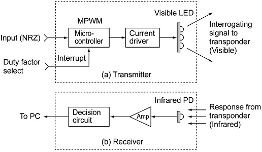
The reader circuit was composed of a transmitter and a receiver, as shown in Fig. 2.
Fig. 2(a) and (b) show the transmitter and receiver circuits, respectively, in the reader. The transmitter consisted of a microcontroller, current driver, and visible light LED array. The receiver was composed of an infrared PD, amplifier, and a decision circuit. When the interrogating signal is applied to the input port, the microcontroller reads the non-return-to-zero (NRZ) interrogating signal and converts it to the MPWM waveform using the duty factor selected by the user. The MPWM signal duty factor can be modified by applying interrupt pulses to the microcontroller. The output voltage of the microcontroller is applied to a current driver, and the visible light from the LED is modulated by the MPWM signal. The output light of the LED array radiates toward the transponder across free space.
When the response signal from the transponder arrives at the reader, it is detected by the infrared PD. The signal is amplified and then passes through a decision circuit. The received data are subsequently sent to the user through a computer. In the reader transmitter circuit, a microcontroller (Atmega328), current driver (DW8501), and 3 × 3 visible light from the LED array composed of nine white LEDs were used. In the reader receiver circuit, an infrared phototransistor (ST5811), an operational amplifier (OPA228), and a buffer (74LS07) for the decision circuit were utilized.
3.2 Modified Pulse Width Modulation (MPWM)
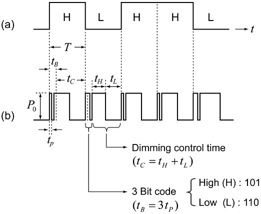
In the transmitter of the reader, the NRZ code of the interrogating signal is transformed into MPWM signals for flicker-free signal transmission and dimming control of visible light from the LED. The conversion from the NRZ into the MPWM waveform is illustrated in Fig. 3.
The waveform of an arbitrary NRZ code and its MPWM waveform are shown in Fig. 3(a) and (b), respectively. The one-bit time of an NRZ bit is T; it is divided into two sections of the three-bit code time, tB, and a dimming control time, tC. The three-bit codes designate the NRZ bit state, and the dimming control time regulates the illumination from the LED. The three-bit codes, (101) and (110), are designated for the high and low bits of the NRZ code, respectively. The one-bit time in the three-bit code is tp thus, the three-bit code time is tB=3tp. The number of high states in a three-bit code is consistently two; it does not change with the NRZ bit states. A dimming control time, tC, is composed of a high state time, tH, and a low state time, tL. The duty factor of the dimming control time can be defined as follows.
| (1) |
The average optical power density of visible light from the LED depends on the duty factor; the illumination is controlled by varying this factor.
3.3 Dimming Control Using Duty Factor
The light from the LED in the reader is modulated by the MPWM signal, and illumination is regulated by the duty factor of the dimming control time in the MPWM waveform. The duty factor is selected by applying the interrupt pulse to the microcontroller in the reader transmitter. The microcontroller is programmed such that the duty factor increases stepwise by 10% for each interrupt pulse from 20% to 90% sequentially. The average optical power density of the light from the LED can be calculated as follows:
| (2) |
where T is the one-bit time of the NRZ code; P0 is the optical amplitude; tp is the one-bit time of the three-bit code; tC is the dimming control time; tH is the duration of the high state in the dimming control time; and Dc is the duty factor of the dimming control time. The average optical power density of the light from the LED does not change with the NRZ bit states. It is unaffected regardless of whether data are transmitted because the number of high states in the three-bit code is independent of the NRZ bit states; its number is consistently two. The average optical power density linearly varies with the duty factor, Dc. Thus, the light from the LED can be regulated by changing the duty factor. To ensure the performance of the dimming control function, a character “Q” was repeatedly transmitted, and the duty factor was increased by 10% stepwise from 20% to 90%. The signal waveforms in the reader transmitter were observed using an oscilloscope, as shown in Fig. 4.
Waveforms observed in reader: (a) NRZ code waveform; MPWM waveforms with duty factors of (b) 20%, (c) 50%, and (d) 90%.
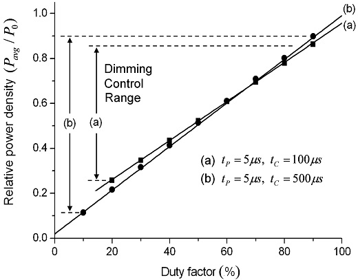
The NRZ waveform of the character, “Q,” in which the one-bit time is 115 μs is shown in Fig. 4(a). The MPWM waveforms with duty factors of 20%, 50%, and 90% are shown in Fig. 4(b)-(d), respectively. In the MPWM waveforms, the one-bit time of the three-bit code was tp=5 μs; thus, the three-bit code time was tB=15 μs, and the dimming control time; was tC=100 μs. In this case, the lower limit of the duty factor can be set to 20%. This is because as the duty factor approaches 10%, the high state of the dimming control time may be confused with the three-bit code, (110), when it is detected by the transponder. The average optical power density of the light from the LED is measured at a distance of approximately 2 m from the LED array to allow for the step-wise change of the duty factor. The relationship between the average optical power density of light from the LED and the duty factor of the dimming control time is shown in Fig. 5.
The solid lines shown in Fig. 5 represent the calculation results of equation (2); the symbols ■ and ● represent the measured values. In the calculation and measurements, the bit time in the three-bit code, tp, was fixed to 5 μs. The values of the dimming control time, tC, were (a) 100 μs and (b) 500 μs. The average optical power density of the LED array linearly increased with the duty factor, as shown in Fig. 5. The dimming control ranges were approximately (a) 26–86% and (b) 11–90% of the constant wave (CW) light from the LED. The CW optical power density was approximately P0=0.2W/m2, corresponding to approximately 230 lx of illumination. The optical power density and illumination provided by the LED were measured using an optical multi-meter (OMM-6810B) and an illuminance meter (UT382), respectively.
4. TRANSPONDER
4.1 Transponder Circuit
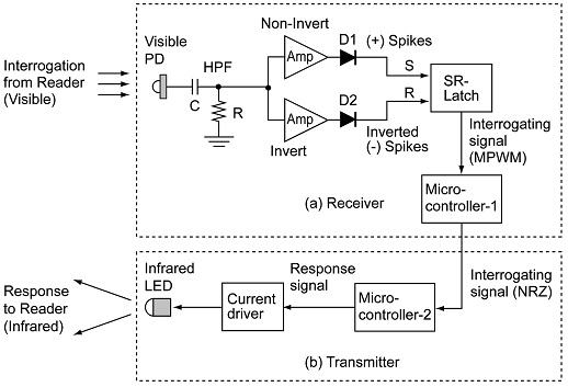
The transponder detects the interrogating signal transmitted by the LED visible light radiated by the reader and sends the response signal to the reader. The configuration of the transponder is illustrated in Fig. 6.
The visible light receiver and infrared transmitter are shown in Fig. 6(a) and (b), respectively. The visible light PD in the receiver detects and receives the signal from the reader. The PD may be exposed to the noise light radiating from adjacent lighting lamps. Generally, the lamps driven by a 60-Hz power line emit noise light with a frequency of 120 Hz. If the noise strength is not negligible when compared with that of the signal light from the reader, then the transponder must be capable of preventing noise interference. A resistor–capacitor (RC) HPF was used for eliminating the noise and spikes in the HPF output was utilized to recover the interrogating signal. If the recovered signal matches the predefined interrogating signal, the transponder generates the response signal and sends it to the reader by modulating the infrared LED.
4.2 Signal Detection Using Spikes
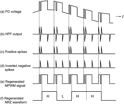
The signal detection process in the transponder is illustrated in Fig. 7.
An example of the PD simultaneously exposed to the signal light from the reader and the 120-Hz noise light from the adjacent lighting lamps is shown Fig. 7(a). These two components are added to the PD voltage. When the PD voltage passes through the HPF, the noise is cut off by the filter. However, the rectangular signal waveforms are also distorted owing to the differential operation of the HPF. When these distorted waveforms are directly read by the microcontroller, the slope of the voltage level can generate errors. To resolve this problem, the spikes in the HPF output are utilized to regenerate the signal waveforms.
When the PD voltage passes through the RC HPF, the 120-Hz noise is cut off. Moreover, positive and negative spikes appear at the leading and trailing edges of the rectangular waveforms, as shown in Fig. 7(b), respectively. The spikes are simultaneously applied to the inputs of the non-invert and invert amplifiers, as shown in the transponder circuit shown in Fig. 6. The output of the non-invert amplifier passes through a diode, D1 only the positive spikes appear in the output of this diode. In contrast, the negative spikes are cut off, as shown in Fig. 7(c). Simultaneously, the output of the invert amplifier passes through a diode, D2 only the inverted negative spikes appear in the output of this diode. In contrast, the positive spikes are cut off, as shown in Fig. 7(d). Thus, the positive and negative spikes are split and separately applied to the set (S) and reset (R) inputs of the SR latch circuit, respectively.
The SR latch output transits to the high voltage at each positive spike and transits to the low voltage at each inverted negative spike. Consequently, the MPWM waveform is regenerated, as shown in Fig. 7(e). The regenerated MPWM signal in the SR latch output is applied to the input of microcontroller-1. This microcontroller executes an interrupt operation at each rising edge of the MPWM signal and sequentially reads the voltage three times at an interval of 5 μs. If the read data are those of (101), the microcontroller outputs high voltage, and the high state continues until the (110) read data appear. If the read data are those of (110), the microcontroller output transits to the low state, which continues until the (101) read data appear. As a result, the NRZ data are recovered, as shown in Fig. 7(f). The recovered NRZ signal is applied to microcontroller-2 to check if it is an interrogating signal. If the recovered NRZ data are equal to the character “Q,” which is defined as the interrogating signal, a response signal to the reader is generated. The voltage waveforms in the transponder are observed with using an oscilloscope, as shown in Fig. 8.
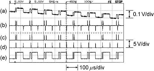
Waveforms observed in transponder: (a) PD voltage, (b) HPF output, (c) positive spikes, (d) inverted negative spikes, and (e) regenerated MPWM waveforms.
The PD voltage when a character “Q” is transmitted by the reader is shown in Fig. 8(a). The slope of the MPWM waveform results from the 120-Hz noise generated by the adjacent lighting lamps. When the PD voltage is applied to the RC HPF, positive and negative spikes appear in the filter output, as shown in Fig. 8(b). The spiked voltage is simultaneously applied to the inputs of the non-invert and invert amplifiers. The positive spikes observed in the outputs of diode D1 are shown in Fig. 8(c), and the inverted negative spikes in the outputs of diode D2 are shown in Fig. 8(d). When the positive and inverted negative spikes are applied to the input S and R of the SR latch, respectively, the MPWM signal is regenerated, as shown in Fig. 8(e).
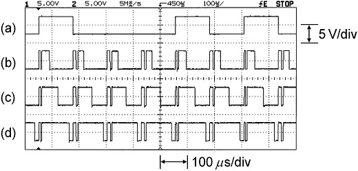
The regenerated MPWM signal was applied to microcontroller-1. At each rising edge of the MPWM signal, the microcontroller executed the interrupt routine in which the voltage was sequentially read three times with 5 μs period from the rising edge. At the instant that the read data corresponded to those of (101) and (110), the output transitioned to high voltage and low voltage, respectively. The output voltage of microcontroller-1 is the same as the NRZ data transmitted by the reader. The NRZ waveform is regenerated in the transponder when the duty factor of the MPWM signal is modified in the reader. The voltage waveforms observed in the transponder using an oscilloscope are shown in Fig. 9.
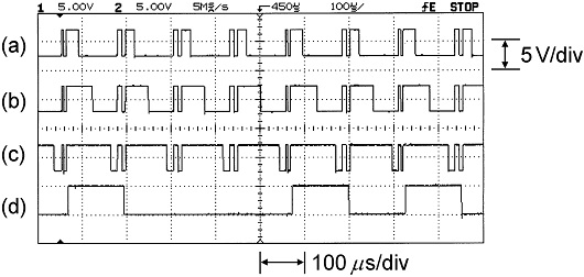
Waveforms observed in transponder: Regenerated MPWM waveforms with duty factors of (a) 20%, (b) 50%, and (c) 90%; (d) Regenerated NRZ code waveform.
The MPWM waveforms regenerated in the transponder with duty factors of 20%, 50%, and 90% are shown in Fig. 9, (a)–(c), respectively. The recovered NRZ code waveform in the transponder is shown in Fig. 9(d). When the duty factor is modified, the shape of the recovered NRZ code remains the same because this code is determined only by the three-bit codes in the MPWM signals. Moreover, it is not affected by the change in the duty factor of the dimming control time.
4.3 Spike Amplitude Change with Capacitance
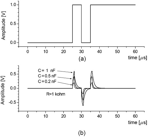
In the transponder circuit, the spikes are employed to regenerate the transmitted interrogating signal. The spike shape depends on the circuit parameters of the RC HPF. The output voltage of the RC HPF is simulated using the PSpice program to find the optimal capacitance values at which the positive and negative spikes have the largest and equal amplitudes; Fig. 10 shows the simulation results.
The input voltage waveform corresponding to the three-bit code, (101), in the MPWM signal, which denotes a high NRZ bit, is shown in Fig. 10(a). The one-bit time of the three-bit code is 5 μs; thus, the shortest pulse width is 5 μs. The simulated output voltage with capacitance values of C = 1, 0.5, and 0.2 nF with the resistance fixed at R=1 kΩ are shown in Fig. 10(b); the spike amplitude varies with the capacitance. The simulation results indicating the variations in the positive and negative spike amplitudes with capacitance are shown in Fig. 11.
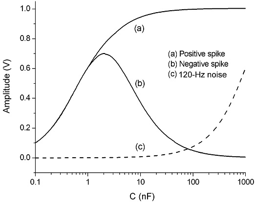
Simulated amplitude variation with capacitance (C): (a) positive spike, (b) negative spike, and (c) 120-Hz noise.
In Fig. 11, curves (a), (b), and (c) are the positive spike, negative spike, and 120-Hz noise amplitudes, respectively. These are in the output of the RC HPF when the input amplitudes of the MPWM signal and the 120-Hz noise amplitudes are set to 1 V. The simulation results showed that the positive and negative spike amplitudes were virtually equal, and the 120-Hz noise disappeared when the capacitance, C, was approximately 1 nF. Thus, in the experiments, C=1 nF and R=1 kΩ were considered for the transponder circuit.
4.4 Response Signal Transmission
Microcontroller-2 in the transponder receives the regenerated NRZ data from microcontroller-1. If the received data match the character “Q,” then microcontroller-2 generates a response signal. The response signal represents the data corresponding to the object to which the transponder is associated for identification. In the experiments conducted, a string character “\tOPID-123\r\n” was used in the response signal. Microcontroller-2 generated the ASCII code corresponding to the response signal. The infrared LED was modulated by the response signal, and the output light radiated to the reader. The infrared response signal was detected using an infrared PD in the reader. The signals in the transponder and reader were observed using an oscilloscope. The voltage waveforms observed in the transponder and reader are shown in Fig. 12.
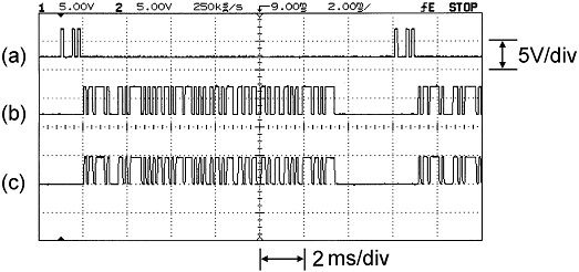
Observed waveforms in transponder and reader: (a) NRZ interrogating signal recovered in transponder, (b) response signal generated by transponder, and (c) response signal received by reader.
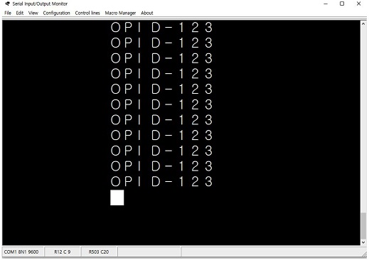
The NRZ interrogating signal received by microcontroller-2 is shown in Fig. 12(a). The interrogating signal was sent repeatedly over a period of 15 ms. The waveform of the response signal generated by microcontroller-2 is shown in Fig. 12(b). The response signal is the string character “\tOPID-123\r\n” in the universal asynchronous receiver–transmitter format at a data rate of 9.6-kbps. The voltage waveforms of the response signal received by the infrared PD in the reader are shown in Fig. 12(c). The received response signal is sent to a personal computer, and the characters are displayed on the monitor, as shown in Fig. 13.
Among the characters in the response signal “\tOPID-123\r\n” sent by the transponder, “\t,” “\r,” and “\n,” are special characters for position control on the monitor. The remaining characters in “OPID-123” are those displayed on the monitor, as shown in Fig. 13.
4.5 Circuits Used in Experiments
The circuit boards used in the experiments are shown in Fig. 14.
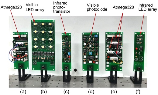
Circuit boards used in experiments: (a) Atmega328, (b) visible LED array, (c) infrared PD, (d) visible PD, (e) Atmega328, and (f) infrared LED array circuits.
The circuits used in the reader, specifically the microcontroller (Atmega328 circuit), visible light LED array, and infrared phototransistor (ST5811 circuit) are shown in Fig. 14(a)-(c), respectively. Those employed in the transponder are shown in Fig. 14(d)-(f). The transponder circuit, including a silicon PIN photodiode (BPW-34), an RC HPF, two diodes (1N4148), an operational amplifier for the invert and non-invert amplifiers (OPA228), and an SR latch, is shown in Fig. 14(d). The two microcontroller circuits (Atmega328) and the infrared LED array in the transponder are shown in Fig. 14, (e) and (f), respectively.
5. CONCLUSION
In this study, we developed an optical identification system with a dimming control function for the visible light from the LEDs. The interrogating signal from the reader to the transponder was transmitted using the visible light modulated in the MPWM waveform. In contrast, the response signal from the transponder to the reader was sent using infrared. In this system, the visible LED array in the reader was used for illumination and interrogating signal transmission. The illumination was regulated by changing the duty factor of the dimming control time in the MPWM signal. In the experiments, we used 15 μs for the three-bit code time and 100 μs for the dimming control time in the MPWM signal. The dimming control range was measured to be approximately in the range of 26–80% of the CW light when the duty factor of the dimming control time was varied from 20% to 90%. In the transponder, the spikes of the RC HPF were utilized to regenerate the interrogating signal while cutting off the 120-Hz noise from adjacent lighting lamps.
This configuration can be used for fabricating optical identification systems for automatic charge calculation or vehicle check at tollgates or parking facilities employing the light from an LED lamp.
Acknowledgments
This study was supported by the Research Program funded by the SeoulTech (Seoul National University of Science and Technology).
REFERENCES
-
X. Ma, K. J. Lee, and K. S. Lee, “Appropriate modulation scheme for visible light communication systems considering illumination”, Electron. Lett., Vol. 48, No. 18, pp. 1137-1139, 2012.
[https://doi.org/10.1049/el.2012.2195]

-
C. Yao, Z. Guo, G. Long, and H. Zhang, “Performance Comparison among ASK, FSK and DPSK in Visible Light Communication”, Opt. Photonics J., Vol. 6, No. 8B, pp. 150-154, 2016.
[https://doi.org/10.4236/opj.2016.68B025]

-
A. M. Cailean and M. Dimian, “Current Challenges for Visible Light Communications Usage in Vehicle Applications: A Survey”, IEEE Commun. Surv. Tutor., Vol. 19, No. 4, pp. 2681-2703, 2017.
[https://doi.org/10.1109/COMST.2017.2706940]

-
V. P. Rachim, Y. Jiang, H. S. Lee, and W. Y. Chung, “Demonstration of long-distance hazard-free wearable EEG monitoring system using mobile phone visible light communication”, Opt. Express, Vol. 25, No. 2, pp. 713-719, 2017.
[https://doi.org/10.1364/OE.25.000713]

-
X. Qiu, J. Wei, J. Li, C. Li, and C. Wei, “A novel identification system based on visible light communication”, Proc. Wirel. Opt. Commun. Conf., pp. 649-652, Chongqing, China, 2013.
[https://doi.org/10.1109/WOCC.2013.6676455]

-
B. Purahong, T. Anuwongpinit, and J. Dumrong, “Identity checking system by visible light”, Proc. 4th Joint Int. Conf. Inf. Commun. Technol. (JICTEE), pp. 1-5, Chiang Rai, Thailand, 2014.
[https://doi.org/10.1109/JICTEE.2014.6804109]

-
S. H. Lee, “A passive transponder for visible light identification using a solar cell”, IEEE Sens. J., Vol. 15, No. 10, pp. 5398-5403, 2015.
[https://doi.org/10.1109/JSEN.2015.2440754]


