Improved Responsivity of an a-Si-based Micro-bolometer Focal Plane Array with a SiNx Membrane Layer
This is an Open Access article distributed under the terms of the Creative Commons Attribution Non-Commercial License(https://creativecommons.org/licenses/by-nc/3.0/) which permits unrestricted non-commercial use, distribution, and reproduction in any medium, provided the original work is properly cited.
Abstract
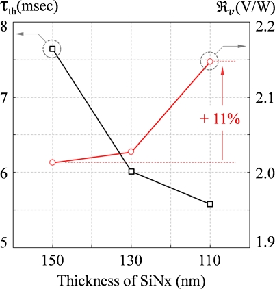
A 12 μm pixel-sized 360 × 240 microbolometer focal plane array (MBFPA) was fabricated using a complementary metal-oxide-semiconductor (CMOS)-compatible process. To release the MBFPA membrane, an amorphous carbon layer (ACL) processed at a low temperature (<400 °C) was deposited as a sacrificial layer. The thermal time constant of the MBFPA was improved by using serpentine legs and controlling the thickness of the SiNx layers at 110, 130, and 150 nm on the membrane, with response times of 6.13, 6.28, and 7.48 msec, respectively. Boron-doped amorphous Si (a-Si), which exhibits a high-temperature coefficient of resistance (TCR) and CMOS compatibility, was deposited on top of the membrane as an IR absorption layer to provide heat energy transformation. The structural stability of the thin SiNx membrane and serpentine legs was observed using field-emission scanning electron microscopy (FE-SEM). The fabrication yield was evaluated by measuring the resistance of a representative pixel in the array, which was in the range of 0.8–1.2 Mohm (as designed). The yields for SiNx thicknesses of SiNx at 110, 130, and 150 nm were 75, 86, and 86%, respectively.
Keywords:
Microbolometer, Responsivity, Thermal heat capacitance, Thermal conductance, Thermal time constant1. INTRODUCTION
Long-wavelength infrared (LWIR) is an electromagnetic wave with a wavelength range of 8–14 μm and provides additional information on visible light, such as thermal energies. In addition, LWIR can be used to provide penetrating images of objects owing to its long wavelengths. Based on these characteristics, LWIR rays are used in various industries and military applications.
Two types of LWIR detection sensors exist: photon- and thermal-detecting sensors. Photon-detection sensors generally have a fast reaction rate and inherit a cooling system to prevent the generation of charge carriers by heat. In contrast, thermal detection sensors detect changes in temperature by absorbing incident infrared radiation. Microbolometers are promising thermal detection sensors that have been extensively investigated. An improved reaction rate was achieved by adopting a modified membrane structure. T. Kim et al. presented a microbolometer with a 16% thermal time constant by patterning holes on a membrane. Chen et al. developed an ultrafast microbolometer using a nanomembrane and attempted to minimize the pixel size to obtain high-resolution images [1, 2].
Owing to its reduced active fill factor, a minimized microbolometer tends to produce high-resolution thermal images by sacrificing the responsivity to LWIR [3, 4]. To compensate for the responsivity of a smaller fill factor, an advanced design of a microbolometer was studied with its membrane structure and optimized leg width and length [5]. A smaller thermal conductance provides a higher responsivity to the microbolometer; however, the minimized thermal conductance limits the frame rate. A high-responsivity microbolometer with a thermal time constant at a high frame rate of over 30 Hz or 60 Hz, depending on the imaging system, is desirable.
While the pixel size and material of the membrane are limited by the complementary metal-oxide-semiconductor (CMOS) integration process, the thickness of the membrane can be exploited to improve thermal performance. In this study, the thermal conductance was controlled by varying the thickness of the microbolometer membrane, and the thermal conductance and fabrication yields of the membranes were compared.
2. DESIGN OF MICROBOLOMETER
According to the responsivity equation shown in Equation (1), the responsivity can be controlled by the bias voltage and temperature coefficient of resistance, thermal conductance, and thermal time constant.
| (1) |
where is the responsivity, VB is the bias voltage, RB is the resistance of the microbolometer, α is the temperature coefficient of resistance (TCR), η is the LWIR absorption, fR is the frame rate, τth is the thermal time constant, and Gth is the thermal conductance.
For a high frame rate, the thermal time constant (τth) should be minimized while maintaining high responsivity. The thermal time constant is shown in equation (2) below.
| (2) |
Thermal capacitance (Cth) is defined as the volume of the membrane with stacked layers comprising different materials. Consequently, the thermal capacitance of the microbolometer is the sum of the specific thermal capacity of each layer (Cp,k) and can be calculated using Equations (3) and (4).
| (3) |
| (4) |
where Cp,K is the specific thermal capacity of the layer, δK is the density of the layer, and υK is the volume of the layer.
The sum of the thermal conductances of a microbolometer is given by Equations (5) and (6).
| (5) |
| (6) |
where NLeg is the number of legs, L is the length of the leg, W is the width of the leg, and t is the layer thickness.
3. FABRICATION OF MICROBOLOMETER
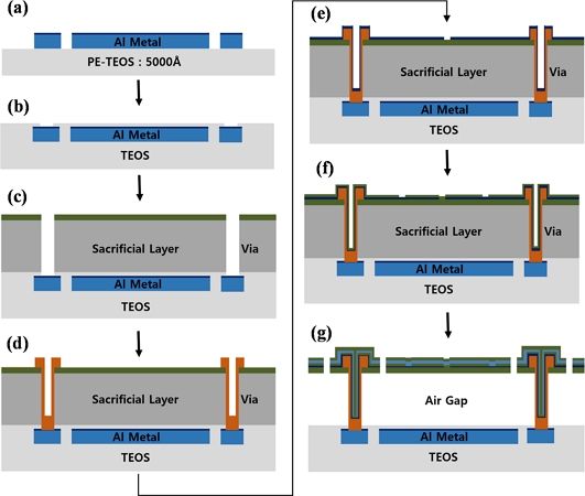
A microbolometer detector with a 360 × 240 microbolometer focal plane array (MBFPA) of 12 μm pixels was integrated using an amorphous silicon material compatible with a CMOS process. Fig. 1 shows a schematic illustration of the fabrication process flow for a microbolometer unit pixel with an air gap. To maximize LWIR absorption within the membrane, the pixel includes an IR-sensitive layer of boron-doped amorphous Si (a-Si) at an incident wavelength λ, isolated thermally from the reflective mirror. First, the bottom mirror and lower electrode metal layer of Ti/Al/TiN with thicknesses of 10/800/15/2 nm were deposited using sputtering equipment (Endura 5500, AMAT) and patterned by etching on the SiOx/Si substrate. The dielectric layer was deposited by a plasma-enhanced chemical vapor deposition (PECVD, P-5000, AMAT) system using a tetra-ethyl-ortho-silicate (TEOS) source, while 200-nm thick SiOx remained on the metal after chemical-mechanical polishing (CMP, Unipla 231, Doosan DND). A sacrificial amorphous carbon layer (ACL) with 1.2 μm thickness was deposited by PECVD [6]. A sub-passivation layer with SiNx was deposited on the ACL sacrificial layer and patterned by a reactive ion etch (RIE, SCCM, TEL) system to open a 1.4 × 1.4 μm via hole through passivation of SiNx, the sacrificial layer, and SiOx on the pad metal. A 300-nm-thick TiN layer, used as an anchor metal, was plated to fill the via holes to electrically connect the thermistors and the readout integrated circuit (ROIC). An absorption layer of 15 nm TiN was then deposited by sputtering with a patterned spacing of 400 nm to meet the target resistance of the bolometer pixel. To fabricate a membrane with a co-planar structure, a 30 nm SiNx layer was deposited to be structurally shared by the thermistor and electrode (absorber) [7]. This process is followed by the deposition of a 100 nm boron-doped a-Si layer as the temperature sensing material with -2.56%/Κ (at 293 Κ), serving as the thermistor element of the bolometers. An additional passivation layer of PECVD SiNx was deposited to achieve a sandwich structure, and the last masking with a dry etching step defined the serpentine leg and bolometer membrane. The final step involved removing the ACL sacrificial layer using O2 plasma stripping to suspend the microbolometer structure [8].

Integration schematic of the mask steps in a-Si microbolometer process flow. (a) Top metal(Al) deposition and patterning, (b) Pad metal opening, (c) Via patterning, (d) Anchor: TiN sputtering, (e) deposition of IR absorption layer (TiN), (f) Nitride deposition, and (g) cantilever patterning and removal of sacrificial layer.
The thicknesses of the passivation layers between the bottom and top layers were 150, 130, and 110 nm, respectively, thus creating a thinner bolometer membrane with lower heat capacity that can be used to minimize the thermal bolometer conductance.
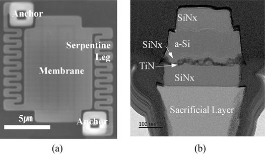
The fabricated microbolometer is shown in Fig. 2. The anchors, serpentine legs, and membranes were well-defined, as shown in Fig. 2(a). Fig. 2(b) shows a cross-sectional FE-TEM image of the serpentine leg. Using a sandwich structure of SiNx/TiN/ SiNx/a-Si/SiNx, the structure was more robust to the residual stress of the layers. As the optimized thickness of a-Si was fixed, the thicknesses of the bottom and top SiNx layers were only varied to reduce Cth and increase microbolometer responsivity.

FE-SEM and FE-TEM views of integrated microbolometer figure; (a) Top view image of a 12? pixel, (b) Cross-sectional view of serpentine leg (FE-TEM image).
Fig. 3 shows FE-SEM images of the three membrane stacks deposited by PECVD SiNx: bottom and top SiNx layers with thickness of 150 nm (volume ratio of 100%), 130 nm (volume ratio of 82%), and 110 nm (volume ratio of 68%), respectively.

Cross-sectional FE-SEM images for microbolometers with thickness of SiNx (a) 150 nm, (b) 130 nm, and (c) 110 nm.
The pixel size was scaled down using the via hole, membrane film thickness, and leg width. Notably, the manufacturing process requirements should be considered to improve the yield of small pixels with uniformity and productivity.
4. CHARACTERIZATION OF MICROBOLOMETER
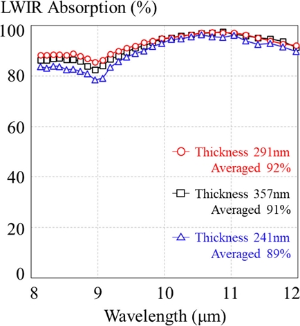
To evaluate the fabricated bolometers, the device was mounted in a vacuum chamber, which was evacuated using a turbo pump to extract its thermal parameters. The proposed bolometer design with 12 μm pixels of 360 x 240 arrays had a fill factor of 54.6% (size of pixels divided by active area). Fig. 4 shows the absorption spectrum of the membrane obtained using Fourier-transform infrared (FTIR) spectroscopy. In a range of 8–12 μm wavelength, the three-layer stacks showed no meaningful absorbance difference to the wave (~8%).

Measured spectrum for a microbolometer structure with the deposition of SiNx with 150 nm, 130 nm, and 110nm, respectively.
The thermal conductance, thermal heat capacitance, and responsivity of the microbolometer with electrothermal characteristics were calculated using Equation (1). Some of the key characteristics of the microbolometer with the SiNx thickness of membrane passivation are summarized in Table 1.
The thermal conductance (Gth) should be lowered as much as possible to maximize bolometer responsivity. However, this lowering is limited by the requirement to maintain a sufficiently small time constant (τth) to make the bolometer compatible with the image frame rate defined by the thermal image system. The typical value of the thermal time constant of the microbolometer is also determined by the thermal mass (Cth) of the absorbing membrane pixel and the heat conductivity, according to equation 2 [9]. Thus, a microbolometer requires a finite-thickness membrane layer to reduce thermal mass.
Fig. 5 shows the responsivity of the microbolometer for a thin SiNx layer with a reduction in thermal mass, with the thermal constant time maintained without significant degradation.
5. CONCLUSIONS
To improve the responsivity of the MBFPA, the thermal conductance and thermal capacitance were deduced using a thin SiNx layer without harming other figures of merit for the MBFPA. While thinner membrane stacks give higher responsivity without a loss of the thermal time constant, they provide lower MBFPA yields due to the fragile structure of the thin membrane; in particular, a membrane thickness of 241 nm shows a similar absorbance to LWIR.
Acknowledgments
This work was supported by the Nanomedical Devices Development Project of NNFC in 2022 (No. 1711160154) and by a National Research Council of Science & Technology (NST) grant (No. CRC-19-02-ETRI) funded by the Ministry of Science and ICT of Korea.
REFERENCES
- T. Kim, J. Oh, J. Park, H. Kim, and Lee JK, “Variation in IR Absorption Characteristics of a Bolometer by Resistive Hole-array Patterns”, J. Sens. Sci. Technol., Vol. 27, No. 5, pp. 306-310, 2018.
-
C. Chen, C. Li, S. Min, Q. Guo, Z. Xia, D. Liu, Z. Ma, and F. Xia, “Ultrafast Silicon Nanomembrane Microbolometer for Long-Wavelength Infrared Light Detection”, Nano Lett., Vol. 21, No. 19, pp. 8385-8392, 2021.
[https://doi.org/10.1021/acs.nanolett.1c02972]

- C. Li, G. Skidmore, C. Howard, E. Clarke, and C. Han, “Advancement in 17-micron pixel pitch uncooled focal plane arrays”, Proc. of SPIE, Vol. 7298, pp. 278-288, 2009.
-
T. Kim, K. Kyung, J. H. Park, Y. S. Kim, S. K. Lim, K. Kim, K. Lee, C. Welham, and H. Y. Kim, “Development of microbolometer with high fill factor and high mechanical stability by shared-anchor structure”, Proc. Of SPIE, Vol. 8353, pp. 454-460, 2012.
[https://doi.org/10.1117/12.918916]

-
F. Niklaus, C. Vieider, and H. Jakobsen, “MEMS-Based Uncooled Infrared Bolometer Arrays-A Review”, Proc. Of SPIE, Vol. 6836, pp. 125-139, 2007.
[https://doi.org/10.1117/12.755128]

-
Y. S. Kim, T. H. Kim, G. T. Kim, B. T. Lim, S. K. Lim, H. D. Lee, and G. W. Lee, “Uncooled Microbolometer Arrays with High Responsivity Using Meshed Leg Structure”, IEEE Photonics Technol. Lett., Vol. 25, No. 21, pp. 2108-2110, 2013.
[https://doi.org/10.1109/LPT.2013.2281623]

-
P. Ericssoon, A. C. Fisher, F. Forsberg, N. Roxhed, B. Samel, S. Savage, G. Stemme, S. Wissmar, O. Oberg, and F. Niklaus, "Towards 17? pitch heterogeneously integrated Si/SiGe quantum well bolometer focal plane arrays", Proc. SPIE, Vol. 8012, pp. 411-420, 2011.
[https://doi.org/10.1117/12.883827]

-
J. S. Oh, H. S. Song, J. C. Par, and J. K. Lee, “Noise Improvement of a-Si Microbolometers by the Post-Metal Annealing Process”, J. Sens., Vol. 21, No. 20, pp. 6722(1)-6722(13), 2021.
[https://doi.org/10.3390/s21206722]

-
J. Y. Jung, K. J. Song, J. H. Choi, J. H. Lee, D. G. Choi, J. H. Jeong, and D. P. Neikirk, “Infrared broadband metasurface absorber for reducing the thermal mass of a microbolometer”, Sci. Rep., Vol. 7, No. 1, pp. 1-8, 2017.
[https://doi.org/10.1038/s41598-017-00586-x]


