Fabrication and Evaluation of Single Layer Graphene/SnO2 Based Gas Sensor for NO2 Detection
This is an Open Access article distributed under the terms of the Creative Commons Attribution Non-Commercial License(https://creativecommons.org/licenses/by-nc/3.0/) which permits unrestricted non-commercial use, distribution, and reproduction in any medium, provided the original work is properly cited.
Abstract
Due to the rapid development of industry, various gases are emitted into the atmosphere, causing environmental pollution and significantly increasing negative health effects on the human body. Among these gases, nitrogen dioxide (NO2) is highly dangerous and can cause various health issues at both low and high concentrations. Severe exposure may even lead to death. Various gas-detection sensors are being developed to detect these gases; however, their effectiveness is limited due to the chemical properties of the gases and environmental factors that affect signal stability. Graphene is a material composed of carbon, known for its excellent chemical properties, low-cost production, and stability at high temperatures as well as in extreme environments. In this study, we synthesized graphene monolayers using low-pressure chemical vapor deposition (LPCVD) and introduced p-type doping with metal oxide tin dioxide SnO2 to enhance its gas-sensing properties. The characteristics of low-concentration NO2 sensing were evaluated, and the impact of temperature changes on sensing performance was analyzed using an internal ceramic heater.
Keywords:
Gas sensors, LPCVD graphene, Oxide semiconductors, SnO2, NO21. INTRODUCTION
Gases produced during the industrial revolution of the 20th century and the rapid development of civilization in the 21st century have had a significant impact on human life. These include carbon monoxide (CO) and carbon dioxide (CO2) from fossil fuels, hydrogen sulfide (H2S) from sewage treatment plants, sewage systems and fertilizer plants, ammonia (NH3) from animal manure, and nitrogen oxides from high-temperature combustion processes in automobiles and power plants. Nitrogen oxides are broadly categorized as nitrogen monoxide (NO), dinitrogen trioxide (N2O3), nitrous oxide (N2O), and nitrogen dioxide (NO2).
NO2 has the greatest impact on human health compared to other nitrogen oxides because it acts as a precursor, reacting with volatile organic compounds (VOCs) to produce ozone (O3). Its health effects vary depending on concentration. Low concentrations of NO2 can cause bronchitis, emphysema, gastrointestinal issues, decreased blood sugar, and increased hemoglobin levels with prolonged exposure. Higher concentrations of NO2 can affect the eyes and respiratory tract, causing coughing, dizziness, vomiting, and headaches. It can even be fatal, leading to pulmonary edema, pneumonia, and increased blood pressure [1-3].
To detect NO2, sensors are being developed using various materials and methods, depending on the operating environment and detection range.
Semiconductor gas sensors detect the target gas through changes in electrical conductivity caused by the interaction of the gas with the surface of a ceramic semiconductor. Electrochemical gas sensors detect the number of electrons (current) generated through oxidation or reduction reactions of the target gas. Contact combustion gas sensors detect the heat generated during the reaction when combustible gases react with oxygen, converting it into an electrical signal. However, there are limitations due to drawbacks such as high operating temperature (> 300°C), interference from gases that should not be measured, and the effects of humidity. In this study, graphene was prepared and used as a NO2 gas sensor.
Graphene has excellent electrical conductivity, low operating temperature, and a large surface area. It has attracted attention in the field of sensors due to its high sensitivity, fast response time, wide sensing range, relatively low production cost, and stability under high temperature and extreme conditions. In 2004, a team of researchers at the University of Manchester in the UK succeeded in producing graphene with a perfect two-dimensional structure at room temperature using a simple mechanical peeling method with Scotch tape and graphite [4]. Although the graphene produced in this way had excellent crystallinity, applying it to sensors for practical applications was challenging due to poor production efficiency, contamination by impurities, and difficulty in controlling the number of graphene layers.
On the other hand, graphene grown by LPCVD has the advantage that the number of graphene layers can be controlled using a metal catalyst such as copper (Cu) foil, high-purity methane, or hydrogen gas, along with the temperature and air pressure inside the chamber. The area of the Cu foil inserted into the chamber can be controlled to produce higher-quality, multifaceted, and high-purity graphene [5].
However, when graphene is only used as a NO2 sensing material, its low sensitivity and selectivity can be an issue. To improve selectivity and sensitivity, SnO2 was used to induce hole migration in the graphene layer.
In this study, we evaluated the characteristics of a graphene/SnO2 gas sensor by growing a single layer of graphene using LPCVD, creating a hybrid material with a metal oxide (SnO2), and estimating changes in the sensing characteristics of the NO2 gas sensor using the proposed gas sensor.
2. EXPERIMENTAL
2.1 Gas sensor fabrication process
The polymethyl methacrylate (PMMA), Isopropyl Alcohol (IPA), deionized water (DI), and acetone used in the experiments were purchased from Sigma-Aldrich, and Cu foil was purchased from Alfa Aesar. All the necessary replacement parts were analytically pure and used directly without further purification.
Field-emission scanning electron microscopy (FE-SEM; SU8030, Hitachi), Raman spectroscopy (InVia Raman Microscope, Renishaw), and X-ray photoelectron Spectroscopy (XPS; Thermo Fisher) were used to evaluate the microstructure and particle size of SnO2 and the number of layers of graphene. Raman spectroscopy was performed using a laser with an excitation wavelength of 532 nm.
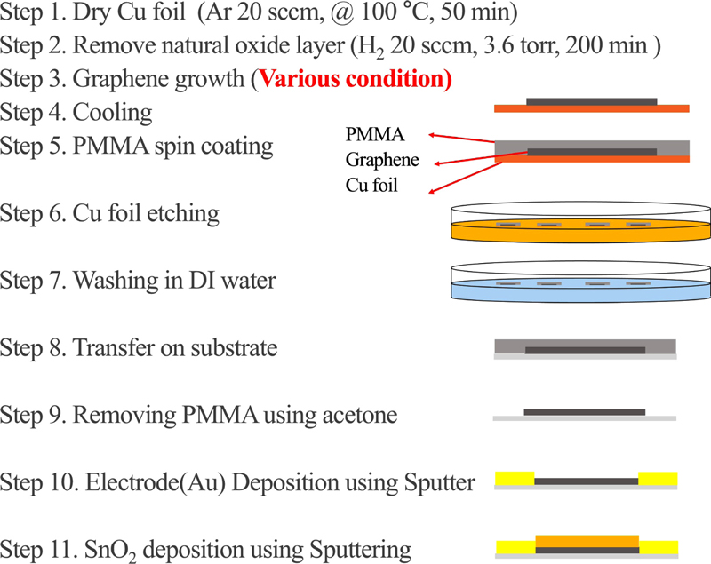
To fabricate graphene, hydrogen (H2, 99.999%), methane (CH4, 99.999%) gas, and Cu or Ni foil are required as metal catalysts. In this study, Cu foil was used to grow graphene. First, Cu foil (Alfa Aesar, USA) was sonicated in acetone, ethanol, and deionized water for 5 min in each solution. Then, the Cu foil was dehydrated using an air gun and placed inside the LPCVD system.
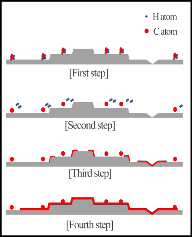
The LPCVD was maintained at 100°C for 20 minutes under 20 sccm of Ar to remove moisture. To remove the oxide layer and impurities on the Cu foil surface, the chamber was heated to 1050°C at a rate of 5 °C/min and pressure was kept at 3.6 torr with 20 sccm of H2. To fabricate graphene by LPCVD, the temperature was maintained at 0.5 torr for 30 minutes, and 500-1000 sccm of CH4 was injected, while maintaining 10 sccm of H2. The decomposition of CH4, which has strong C-H intermolecular bonds, proceeds on the Cu foil, which acts as a metal catalyst. Subsequently, nucleation of graphene occurs at the edges or grain boundaries of the Cu surface, where the activation energy of the hydrocarbons is high. The nucleated carbon atoms diffuse towards the center of the graphene, and the graphene grows. A schematic of this process is shown in Fig. 1. After the graphene growth was completed, cooling was performed with a flow rate of 20 sccm of H2 at a pressure of 6 torr, at a cooling rate of -5°C/min until 600°C and -2.5°C/min thereafter. The two cooling recipes were used to ensure that the crystallinity of the Cu foil itself did not change and that the graphene grown on it was not affected.
The grown graphene was then wet-transferred to poly (methyl methacrylate) PMMA. The PMMA was applied by spin coating onto the Cu foil on which the graphene was grown and then heat treated in a box furnace at 70°C for 30 minutes to induce curing of the polymer. The Cu foil was removed using a Cu etchant and washed three times with deionized water. The graphene was then transferred to a SiO2/Si wafer cleaned with IPA, Acetone, and other heat treatments to remove moisture and wrinkles between the PMMA and graphene. Finally, the residual PMMA was removed by solution treatment in chloroform for 2 h and heat treatment in an H2 atmosphere. This process was performed carefully, as residual PMMA tends to degrade the properties of graphene itself, which in turn reduces the sensitivity of the sensor. A schematic of this process is shown in Fig. 2. To form the electrodes, 20 nm of titanium (Ti) and 200 nm of gold (Au) were deposited using a physical mask and an e-beam evaporator. Ti was deposited to a thickness of 1/10 that of Au, which plays a role in this study as an adhesion layer.
After Step 10 (Fig. 2), SnO2 was deposited to a thickness of about 150 nm by sputtering.
3. RESULTS AND DISCUSSIONS
3.1 Evaluation of Gas Sensor Components
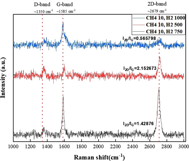
To confirm that monolayer graphene was prepared, Raman spectroscopy of graphene grown on the Cu foil was performed before transferring it to a substrate. Three bands were observed in the Raman spectrum of graphene. The G band, located at 1585 cm-1, is a mode in which the carbon atoms in the hexagonal structure vibrate in the opposite direction to their neighbors and is known to be a co-found peak in graphitic materials. The D band, which appears in the presence of a sp3 crystal structure or defects caused by chemical reactions or other physical treatments, indicates the degree of sample defects and is located at 1350 cm-1. Finally, the 2D band (or G` band), located at 2679 cm-1, is a peak caused by secondary scattering from the emission of two phonons of the D band, which varies greatly with graphene thickness and is used to indicate the number of layers. The 2D/G ratio, shown in Fig. 3, was used to analyze the grown graphene and determine the number of graphene layers. A value less than one indicates multilayer graphene, a value between one and two indicates bilayer graphene, and a value of two or more indicates single-layer graphene [6].
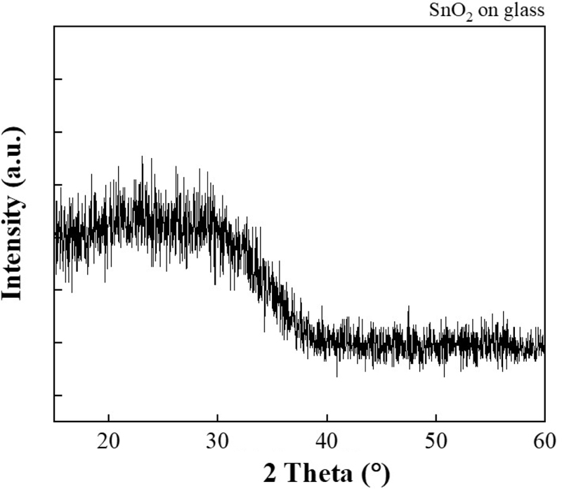
Fig. 4(a) and (b) show that the deposition of SnO2 by sputtering is very fine, with a thickness of approximately 150 nm. The XRD patterns in Fig. 5 also show the presence or absence of SnO2 on the slide glass [7]. A photograph of the fabricated sensor is shown in Fig. 6(a), and it is evident that it was deposited well compared to the schematic in Fig. 6(b). The actual size of the sensor is 0.5 × 1 cm2.
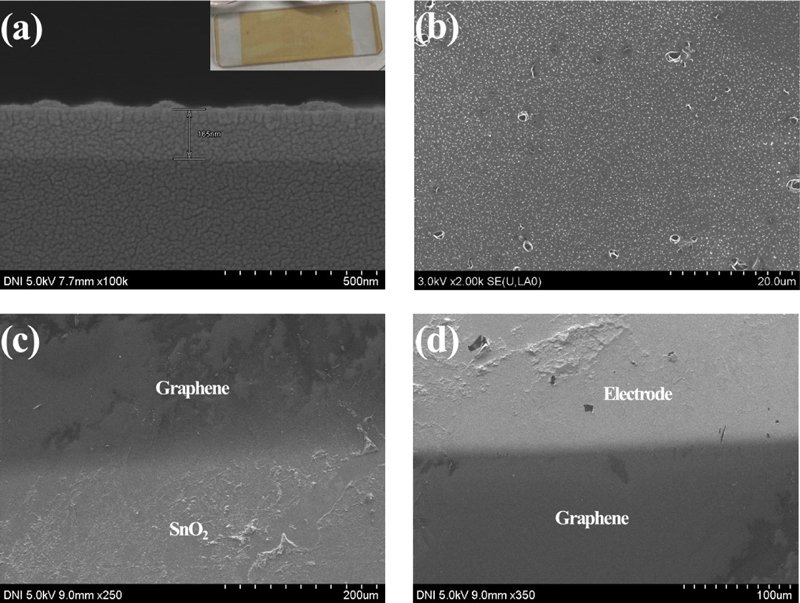
Evaluation of the microstructure of the sensor: (a) Cross-sectional SEM image of slide glass/SnO2, (b) SEM image of the SnO2 region in the hybrid sensor, (c) SEM image of Graphene/SnO2 region in the hybrid sensor, (d) SEM image of the electrode (Au)/Graphene region in the hybrid sensor.
In cases (c) and (d) in Fig. 4, the microstructure of the boundary between graphene/SnO2 and graphene/electrode (Au) shows that a single layer or bilayer of graphene was created by the difference in brightness. Furthermore, it is confirmed that no chemical reaction occurred between the materials [8].
3.2 NO2 gas sensing
Electron transfer in the sensor by NO2 can be expressed by Equations (3) and (4), which are similar to Equations (1) and (2) If the number of h+, the major carrier in graphene that behaves like a p-type, increases, the resistance decreases.
| (1) |
| (2) |
| (3) |
| (4) |
The change in the electrical signal of the graphene sensor in response to NO2 gas was measured using the prepared chamber. Air was used as the reference gas, and the concentration of NO2 gas was varied by adjusting the flow rate inside the chamber. A ceramic heater was placed inside the chamber to measure the sensitivity of the fabricated NO2 sensor at various operating temperatures.
To estimate the sensitivity to NO2, electrical signal change was measured by repeatedly introducing 10 ppm of NO2 into the chamber. The electrical signal change caused by temperature changes was also measured through the ceramic heater inside the chamber. The response shown in Figs. 7, 8, 9, 11 are was calculated using equation (5), where Ra is the resistance of the reference gas and Rg is the resistance of the reference gas containing NO2.
| (5) |
Fig. 7 shows the NO2 characteristics of the sensor fabricated using graphene.
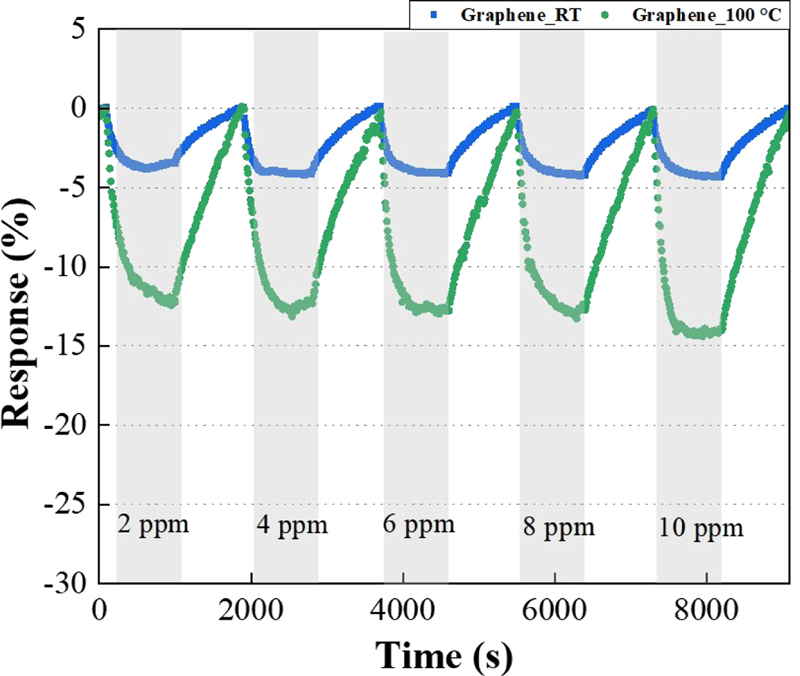
Evaluation of NO2 measurement in gas sensors using graphene as a function of temperature and gas concentration.
As the concentration of NO2 increases, the reactivity of the graphene sensor at room temperature gradually increases to values of -2.4, -4.0, -4.1, -4.2, and -4.3. The graph shows an increase of about 4 times at a temperature of 100°C. However, as mentioned earlier, to ensure selectivity and reactivity, we prepared a sensor with SnO2 deposited on it.
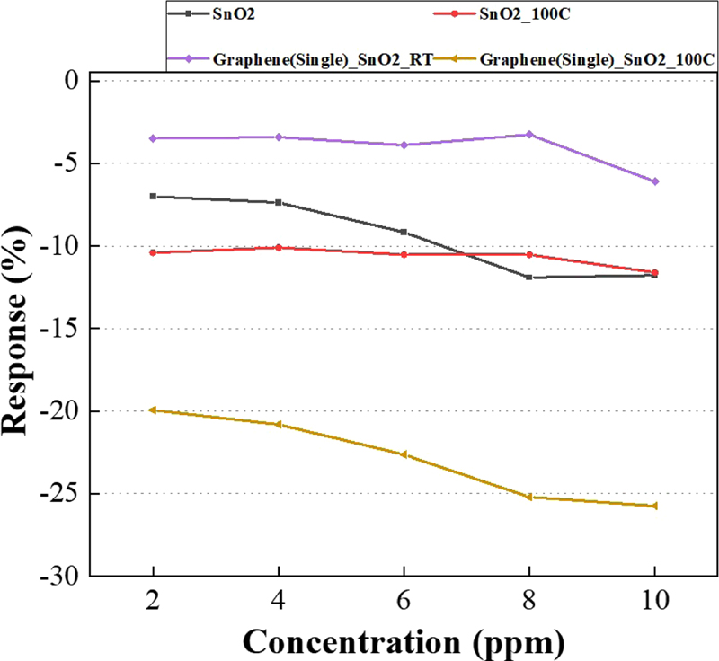
Fig. 8 shows that each sensor detected NO2 gas as its concentration increased from 2 to 10 ppm. The graphene/SnO2 sensor was more responsive than the sensor made of SnO2 alone.
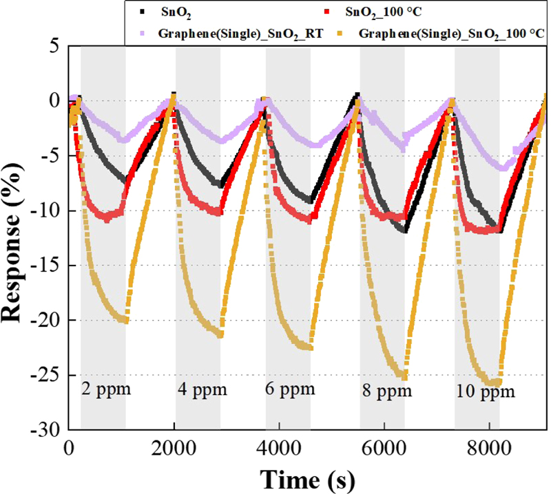
Evaluating the response of gas sensors to NO2 as a function of temperature, material and gas concentration.
When graphene, known for its role as a major carrier of holes in p-type doping materials, and SnO2, a metal oxide, are combined, the electrons on the graphene side are displaced due to the rearrangement of the Fermi level, and the number of holes is increased. The change in resistance caused by NO2 gas was significantly greater in the SnO2/graphene sensor due to the increase in holes compared to the sensors with either SnO2 or graphene alone as the detection material.
The work function of each metal oxide played an important role in this response. The work function of graphene is known to be approximately 4.5 eV [9]. Metal oxides, such as SnO2, which have a work function greater than this value, react more actively with p-type doping.
Thus, a reactivity improvement of about 15% is observed for the graphene/SnO2 sensor compared to the sensor made of SnO2 alone at 100°C.
Fig. 9 shows a graphical representation of the maximum reactivity at each concentration. Among all the sensors, the graphene sensor was the least responsive at room temperature. However, the graphene/SnO2 sensor also shows no increase in reactivity compared with the graphene sensor at room temperature. The highest reactivity was observed at 100°C. This confirmed that the reaction on the metal oxide surface, Equation (1), became more active as the temperature increased, resulting in the highest reactivity when measured at 100°C instead of room temperature.
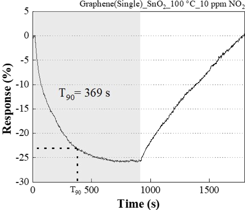
During the experiment, the response time (T90) was calculated from the response graph of the graphene/SnO2 Hybrid sensor to 10 ppm NO2 at 100°C, which is the highest response.
The response time is about 70 seconds.
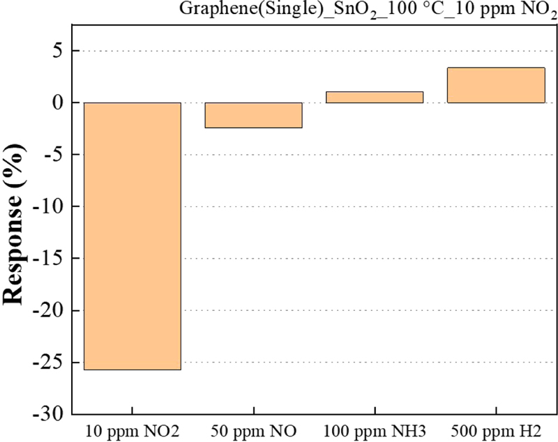
Fig. 11 shows the selectivity evaluation using gases from the NOx family, including NO, NH3 (which is also present in sewage treatment plants, human breath), and H2 gas. Each gas was concentrated to 50 ppm NO, 100 ppm NH3, 500 ppm H2 or 10 ppm NO2.
It is evident that 10 ppm NO2 gas is approximately six times more reactive than gases with higher concentrations. The SnO2 metal oxide helps to improve the reactivity to NO2 gas, resulting in higher selectivity.
4. CONCLUSIONS
In this study, a NO2 sensor using a graphene monolayer fabricated by LPCVD and SnO2 deposited by sputtering was developed to demonstrate improved responsiveness to NO2 gas.
The direct mechanism is that SnO2, whose work function is higher than that of graphene, reduces the Fermi level (EF). This causes a phenomenon similar to higher p-type doping when reacting with gas, thus increasing the responsiveness to NO2 gas. Although this effect is weak at room temperature, at 100°C, the migration of holes on the surface of the metal oxide becomes more active, increasing reactivity. It was confirmed that SnO2 itself exhibits higher selectivity for NO2 compared to other gases, resulting in greater reactivity even when compared with higher concentrations of NO, NH3, and H2.
Acknowledgments
This work was supported by the Technology Development Program (S3366415) funded by the Ministry of SMEs and Startups of Korea (MSS, Korea). Additionally, this study was conducted with the support of the Korea Institute of Industrial Technology under “Development of high-performance pressure sensor for self-diagnosis brake system of hybrid/electric vehicle (Kitech UI-24-0008)”.
REFERENCES
-
G. Pershagen, E. Rylander, S. Norberg, M. Eriksson, and S. L. Nordvall, “Air pollution involving nitrogen dioxide exposure and wheezing bronchitis in children”, Int. J. Epidemiol., Vol. 24, No. 6, pp. 1147-1153, 1995.
[https://doi.org/10.1093/ije/24.6.1147]

-
Z. Zhang, J. Wang, and W. Lu, “Exposure to nitrogen dioxide and chronic obstructive pulmonary disease (COPD) in adults: a systematic review and meta-analysis”, Environ. Sci. Pollut. Res., Vol. 25, pp. 15133-15145, 2018.
[https://doi.org/10.1007/s11356-018-1629-7]

-
S. Miyata, A. Noda, Y. Hara, J. Ueyama, K. Kitaichi, T. Kondo, and Y. Koike, “Nitric oxide plasma level as a barometer of endothelial dysfunction in factory workers”, Exp. Clin. Endocrinol. Diabetes, Vol. 125, No. 10, pp. 684-689, 2017.
[https://doi.org/10.1055/s-0043-110054]

-
K. S. Novoselov and Y. Koike, “Graphene: materials in the flatland (Nobel Lecture)”, Angew. Chem. Int. Ed., Vol. 50, No. 31, pp. 6986-7002, 2011.
[https://doi.org/10.1002/anie.201101502]

-
Z. Ullah, S. Riaz, Q. Li, S. Atiq, M. Saleem, M. Azhar, S. Naseem, and L. Liu, “A comparative study of graphene growth by APCVD, LPCVD and PECVD”, Mater. Res. Express, Vol. 5, No. 3, p. 035606, 2018.
[https://doi.org/10.1088/2053-1591/aab7b4]

- I. Childres, L. A. Jauregui, W. Park, H. Cao, and Y. P. Chen, “Raman spectroscopy of graphene and related materials”, New Developments in Photon Mater. Res., Vol. 1, pp. 1-20, 2013.
-
P. Chetri and J. C. Dhar, “Au/GLAD-SnO2 nanowire array-based fast response Schottky UV detector”, Appl. Phys. A, Vol. 125, pp. 1-8, 2019.
[https://doi.org/10.1007/s00339-019-2590-0]

-
Z. J. Wang, J. Dong, Y. Cui, G. Eres, O. Timpe, Q. Fu, F. Ding, R. Schlögl, and M. G. Willinger, “Stacking sequence and interlayer coupling in few-layer graphene revealed by in situ imaging”, Nat. Commun., Vol. 6, No. 1, p. 13256, 2016.
[https://doi.org/10.1038/ncomms13256]

-
R. Garg, N. K. Dutta, and N. R. Choudhury, “Work function engineering of graphene”, Nanomaterials, Vol. 4, No. 2, pp. 267-300, 2014.
[https://doi.org/10.3390/nano4020267]

