
A Review of Recent Technologies for Temporal Noise Reduction in Mobile CMOS Image Sensors

ⓒ The Korean Sensors Society
This is an Open Access article distributed under the terms of the Creative Commons Attribution Non-Commercial License (https://creativecommons.org/licenses/by-nc/3.0/) which permits unrestricted non-commercial use, distribution, and reproduction in any medium, provided the original work is properly cited.
Abstract
The continuous scaling of pixel sizes in mobile CMOS Image Sensors (CIS) to achieve higher resolutions has posed significant challenges, most notably the degradation of dark performance due to increased temporal noise. This review provides a comprehensive analysis of fundamental noise sources—including thermal, flicker, Random Telegraph Noise (RTN), and leakage currents—that are exacerbated by this scaling trend. It then surveys a range of state-of-the-art technologies developed to mitigate these effects. The discussion covers major technological advancements, such as advanced stacked architectures that decouple photodiode and transistor design; innovative three-dimensional transistor designs, including FinFETs, Bi-gate FETs, and Back-End-of-Line (BEOL) IGZO FETs; techniques for achieving high conversion gain to improve the signal-to-noise ratio; and circuit-level methods like multiple sampling and noise-bandwidth limiting. Finally, this review highlights the emergence of photon-counting sensors, such as Quanta Image Sensors (QIS) and CMOS Photon Detectors (CPD), as a paradigm shift in low-light imaging, demonstrating the industry's trajectory toward overcoming the physical limitations of pixel scaling.
Keywords:
CMOS image sensor, Temporal noise, Dark noise, Pixel transistor1. INTRODUCTION
The primary driver in the mobile CMOS Image Sensor (CIS) market is the persistent demand for higher resolution within increasingly compact camera module form factors. This trend has necessitated aggressive scaling of pixel pitch, with modern sensors featuring pixel sizes that have shrunk from over 1.0 µm to 0.5 µm. However, this relentless miniaturization introduces a fundamental trade-off that directly compromises image quality, particularly in low-light conditions.
As pixels scale down, the photodiode (PD) area and the in-pixel amplifier transistors must be reduced proportionally. This downsizing results in a reduced Full Well Capacity (FWC) and, crucially, a significant elevation in temporal noise. Smaller amplifier transistors exhibit lower transconductance (gm) and smaller channel areas, which directly intensify thermal noise (proportional to 1/gm) and heighten susceptibility to flicker (1/f) noise and Random Telegraph Noise (RTN)—both of which are inversely proportional to the channel area. This degradation diminishes low-light image quality by raising the noise floor and compromising dynamic range.
The purpose of this paper is to provide a comprehensive review of the latest technological advancements and physical mechanisms aimed at mitigating temporal noise in highly scaled CIS pixels. Specifically, this work synthesizes state-of-the-art technologies presented by industry leaders—such as Sony, Samsung, and OmniVision—at premier conferences over the past five years, including the International Solid-State Circuits Conference (ISSCC), the International Electron Devices Meeting (IEDM), the Symposia on VLSI Technology and Circuits, and the International Image Sensor Workshop (IISW). We first analyze the primary noise sources that degrade the signal within the pixel readout chain. Subsequently, we survey key noise-reduction technologies implemented at the device, pixel, and circuit levels, ranging from novel transistor structures to advanced readout architectures. To effectively evaluate these mitigation strategies, it is essential first to understand the fundamental physical origins of the noise.
2. FACTORS INFLUENCING TEMPORAL NOISE IN THE PIXEL READOUT CHAIN
Fig. 1(a) presents a low-light image exhibiting severe temporal noise. Stochastic fluctuations in each pixel's output signal degrade the low-light SNR and dynamic range (DR). In practice, read noise is typically quantified by calculating the multi-frame temporal standard deviation (σmulti-frame) of individual pixel responses across a sequence of dozens of consecutive frames. Effective mitigation of temporal noise requires a comprehensive understanding of its constituent sources within the pixel's readout chain. Each noise component has a distinct physical origin and frequency-domain characteristic. Consequently, a precise diagnosis of these components is critical for developing targeted reduction technologies that address the root causes of performance degradation.
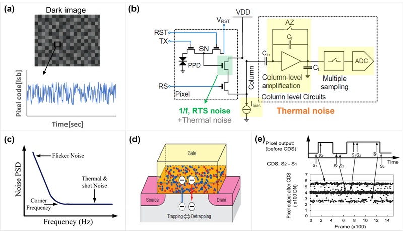
Temporal noise characterization and mechanisms in CIS. (a) Example of a low-light image with severe temporal noise. (b) Major noise sources in the pixel readout chain. Adapted from Ref. [1]. (c) Pixel noise power spectral density (PSD) consisting of 1/f noise and wideband thermal noise. Adapted from Ref. [2]. (d) low-frequency noise generation by Si/SiO2 interface traps in the source follower (SF). Adapted from Ref. [3]. (e) Time-domain RTS waveform exhibiting characteristic discrete, step-like fluctuations. Adapted from Ref. [4].
2.1 Overall Noise in the Readout Chain
Fig. 1(b) illustrates the primary noise sources within the overall pixel readout chain [1]. From a frequency-domain perspective, as shown in Fig. 1(c) [2], the temporal noise present in the pixel readout circuitry is categorized into two primary types:
1) Flicker Noise (1/f noise): This low-frequency component exhibits a power spectral density inversely proportional to the frequency. In modern CIS designs, it is significantly attenuated by the Correlated Double Sampling (CDS) function, which cancels out low-frequency fluctuations by subtracting the reset level from the signal level.
2) Thermal Noise: This is a high-frequency, wideband noise generated by the thermal agitation of charge carriers. Its total integrated power is limited by the operational transconductance amplifier (OTA) in the readout comparator, which has a finite bandwidth (-3 dB cutoff frequency) that acts as a low-pass filter.
The combined transfer functions of these filtering mechanisms effectively shape the final readout noise. Although the CDS (acting as a high-pass filter) and the OTA (acting as a low-pass filter) successfully suppress a substantial portion of the noise, they do not eliminate it. In practice, residual noise components persist, forming a baseline noise floor that significantly deteriorates image quality and the signal-to-noise ratio (SNR), particularly under low-light conditions.
2.2 Thermal Noise
Thermal noise, also known as Johnson-Nyquist noise, is generated by the random thermal motion of charge carriers within the readout transistors- most notably the source follower (SF), the load transistor, and subsequent analog blocks. The voltage spectral density (Svg,thermal) of this noise is defined by the following relationship:
Here, k is the Boltzmann constant, T is the absolute temperature, gm1 and gm2 represent the transconductance of the source follower and the load transistor, respectively, and γ is a process-dependent noise coefficient often influenced by channel length effects. This formula reveals a critical design principle: thermal noise is inversely proportional to the transconductance of the SF. Therefore, a primary and most effective strategy for suppressing thermal noise is to maximize gm1 relative to gm2. Technically, this is achieved by increasing the transistor's channel width or by adopting advanced structures (e.g., FinFETs or stacked pixel architectures), as discussed in later sections.
2.3 Flicker Noise (1/f) and Random Telegraph Signal (RTS)
Flicker Noise, commonly referred to as 1/f noise, is a low-frequency noise component originating from the random trapping and de-trapping of charge carriers at the silicon/silicon dioxide (Si/SiO2) interface of the SF as shown in Fig. 1(d) [3]. Its gate voltage spectral density (Svg,1/f) is described by the McWhorter model:
In this expression, W and L represent the transistor's channel width and length, respectively, q is the elementary charge, λ is the tunneling coefficient, Cox is the gate oxide capacitance per unit area, and Nit denotes the interface trap density. The key implication of this relationship is that flicker noise is inversely proportional to the transistor's channel area (W × L). Therefore, as the interface trap density (Nit) increases or the device dimensions shrink, the 1/f noise power becomes more dominant.
Random Telegraph Signal (RTS), also known as RTN, is a discrete, more severe form of this trapping phenomenon. Unlike the averaged effect of 1/f noise, RTS appears as step-like, multi-level fluctuations in the output signal (Fig. 1(e)) [4]. It is typically caused by a single, dominant defect or trap in the transistor channel that captures and releases individual charge carriers, significantly modulating the channel's conductance.
The impact of pixel scaling is particularly detrimental to these noise sources. As pixel amplifier transistors are scaled down to fit smaller footprints, the significant reduction in channel area (W × L) makes the device far more susceptible to both cumulative flicker noise and the localized effects of single-trap RTS.
2.4 Leakage-Induced Noise and Transistor Reliability Factors
As CIS scales down to sub-micron pixel pitches, transistor reliability has emerged as a critical factor limiting noise performance. Mechanisms such as Hot Carrier Injection (HCI), Gate-Induced Drain Leakage (GIDL), and radiation-induced stress significantly influence the characteristics of RTS [5,6].
HCI is a primary aging mechanism in pixel source followers (SF), where high-energy carriers generate defects at the Si/SiO2 interface. Unlike the threshold voltage (Vth) shift, which tends to evolve uniformly across the pixel population under stress, RTS degradation is inherently discrete and stochastic [7]. Statistical analysis of over one million devices reveals that while the Vth shift correlates linearly with stress time, the RTS distribution exhibits a distinct bifurcation, signifying the stochastic generation of new trap sites. HCI stress can transform previously stable devices into RTS-exhibiting ones. Notably, a significant portion of these stress-induced traps, termed “Soft RTS”, can be recovered through high-temperature annealing (e.g., 240°C), whereas process-induced “Hard RTS” remains unaffected [8].
In addition to SF noise, the reset transistor contributes significantly to the noise distribution tail through GIDL. GIDL-RTS originates from trap-assisted tunneling (TAT) or metastable trap states within the high-field region near the reset gate edge [9]. This noise source is highly sensitive to the gate-to-source voltage (VSG). By increasing the reset-low voltage (VRSTL), the VSG is reduced, effectively suppressing GIDL-RTS and ensuring the SF channel RTS remains the dominant noise component.
Beyond conventional noise mechanisms, exposure to cosmic rays in extreme environments—such as outer space or high-altitude aviation—represents a critical source of noise-induced defects and reliability issues in CIS. These environments subject the sensors to Total Ionizing Dose (TID) and Displacement Damage Dose (DDD), leading to dark signal degradation and Random Telegraph Signal (RTS). Proton irradiation (DDD) creates displacement damage that manifests as hot pixels and DC-RTS with exponentially distributed amplitudes [10]. Gamma irradiation also induces RTS; however, degradation is significantly accelerated when the device is biased during irradiation. Biased conditions exacerbate the formation of interface states, leading to a higher fraction of pixels exhibiting multi-level RTS than in grounded conditions.
2.5 Feedback Noise
During the charge-sensing phase, when the reset transistor is off, the in-pixel SF is subject to a positive feedback mechanism driven by capacitive coupling between the source and the floating gate via the gate-to-source capacitance (Cgs) [11]. This feedback loop, quantified by the factor β = Cgs/Cfd, increases the effective output impedance of the source follower by a factor of (1 + β), which consequently extends the column settling time and can be detrimental to high-speed readout performance. More critically, this phenomenon amplifies the noise voltage at the column; the noise spectral density increases by a factor of (1 + β)2, and the sampled thermal noise deviates from the standard kT/Ccol limit to approximately (1 + β)kT/Ccol, thereby exacerbating all noise components, including thermal, 1/f noise, and RTS. Therefore, minimizing Cgs is essential to suppress noise amplification and ensure high-speed readout.
3. ADVANCED TECHNOLOGIES FOR TEMPORAL NOISE REDUCTION
The image sensor industry has addressed the noise challenges arising from pixel scaling through a multi-faceted approach, driving innovation in device architecture, fundamental transistor physics, and readout circuitry. Collectively, these advancements aim to suppress noise at its source, enhance the signal to surpass the noise floor, or eliminate noise during the readout process.
3.1 Shared Pixel Architectures
To mitigate the degradation of transconductance (gm) and the increase in 1/f noise associated with pixel shrinkage, multipixel-sharing architectures have been widely adopted to maximize the effective area (W × L) of the SF amplifier. By sharing the floating-diffusion (FD) node and readout circuitry across multiple pixels (e.g., 2 × 2 or 2 × 4 clusters), the layout area allocated to the SF transistor is significantly increased. This structural optimization directly suppresses RTS and thermal noise components by reducing the impact of individual interface traps and enhancing gm [12-14]. For instance, in a 0.5 μm-pitch 200MP sensor, a 2 × 4 shared pixel structure utilizing three parallel-connected bending SFs demonstrated a reduction in temporal noise to 1.6. This was achieved by maximizing the effective channel width within the shared layout, proving that architectural synergy can effectively compensate for the physical scaling limits of sub-micron pixels [12].
3.2 High Conversion Gain (CG)
Evaluating noise in terms of input-referred electrons () is essential as it normalizes noise performance across diverse architectures by decoupling it from the sensor's conversion gain. For a given output voltage noise floor, the input-referred noise is inversely proportional to the conversion gain, which is defined as CG = q/CFD, where q is the elementary charge and CFD is the total capacitance at the floating diffusion node. Therefore, minimizing parasitic components in CFD—metal wiring capacitance, junction capacitance, and transistor gate overlap capacitance—is the primary strategy for achieving high-CG performance. Recent literature demonstrates various approaches to minimizing these parasitic components through structural and device engineering [14].
Several techniques are employed to achieve high CG:
1) Locally Lowered-Stack (LLS) Technology: To reduce the metal-to-metal parasitic capacitance in FD sharing structures, a locally lowered-stack (LLS) technology has been proposed [14,15]. As shown in Fig. 2(a), reducing the gate stack height by 40% maximized conversion gain, achieving a low input-referred temporal noise of 1.6 in 0.5 μm pixels [15]. Furthermore, by specifically reducing the height and thickness of the FD metal interconnection (Fig. 2(b)), the coupling capacitance to surrounding metal layers is significantly reduced [14]. Simulations and measurements confirm that LLS reduces CFD by 29%, resulting in a 40% enhancement in CG and a 25% reduction in temporal noise.
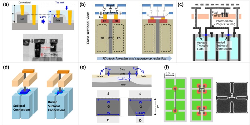
Schematic illustrations of high-CG enhancement strategies. (a) 40% reduction in gate stack height. Adapted from Ref. [15]. (b) Locally lowered metal layers for FD. Adapted from Ref. [14]. (c) IPW for 2-layer stacked routing. Adapted from Ref. [16]. (d) BSC with buried sidewall contacts. Adapted from Ref. [17]. (e) NDSF with asymmetric 33% drain width. Adapted from Ref. [18]. (f) DTI Center-Cut for shared FD clusters. Adapted from Ref. [19].
2) Poly-Si Wiring: In two-layer stacked pixels, deep contacts are typically employed to connect the PD layer to the transistor layer. However, these contacts often impose layout constraints and introduce significant parasitic capacitance. The implementation of Intermediate Poly-Si Wiring (IPW) between the deep contacts and the PD silicon layer enables more flexible routing and reduces the reliance on long, high-capacitance metal interconnects (Fig. 2(c)) [16]. This approach has demonstrated a 24% reduction in wiring-related CFD, contributing to a 72% increase in CG and a 42% reduction in read noise. In addition, while conventional surface wiring for shared FDs adds substantial parasitic capacitance, Buried Sublocal Connections (BSC) further improves CG. By utilizing buried contacts within the silicon sidewalls to interconnect multiple FDs, as shown in Fig. 2(d), BSC effectively mitigates the parasitic capacitance between the FD node and the transfer gates [17]. Experimental results indicate that this method, when combined with optimized FD sharing units, achieves a 46% reduction in CFD and a 2.26-fold increase in CG.
3) Narrow Drain Source Follower (NDSF): The drainside overlap capacitance (Cgd) is a primary contributor to the total parasitic capacitance of the SF. By implementing an asymmetric SF transistor with a narrowed drain width—for instance, reduced to 33% of its original dimension as shown in Fig. 2(e) —the total effective SF capacitance can be lowered to approximately 88% [18]. This structural optimization directly leads to a higher conversion gain (CG) and improved linearity in low-light environments by effectively suppressing short-channel effects.
4) DTI Center-Cut (DCC) for FD Sharing: In Quad-cell or Tetracell structures, removing the Deep Trench Isolation (DTI) at the intersection of four pixels—a technique referred to as DTI Center-Cut—enables the formation of a shared FD region (Fig. 2(f)) [19]. This eliminates the need for complex metal jumpers to interconnect individual FDs, thereby simplifying metal routing and reducing the total junction area. This structural change alone has been reported to increase CG by 38%.
5) Other techniques: To minimize the FD junction capacitance, reducing the FD area is necessary; however, this reduction often risks hindering charge transfer efficiency. Although not primarily designed as a direct CG-enhancement technique, the implementation of a Dual Vertical Transfer Gate (Dual-VTG) indirectly facilitates higher CG by ensuring robust charge transfer even within a minimized FD footprint. This structural synergy enables achieving extreme conversion gain (e.g., 180 μV/e−) while effectively maintaining full well capacity [19].
3.3 Stacked Pixel Architectures
A foundational innovation in modern CIS technology is the stacked architecture. While initial stacked designs focused on separating the pixel array from the logic circuit layer, recent advancements have further bifurcated the pixel layer itself into dedicated PD and pixel-transistor layers. By fabricating the PDs and pixel transistors on separate wafers—separate from the underlying logic—the traditional design constraint in which the PD and transistors compete for the same lateral area is effectively eliminated. This three-dimensional subdivision allows both the PD and the amplifier transistors to be optimized for maximum area and performance [16,20-23].
The decoupling of these layers has a profound impact on noise reduction. It allows for increased transistor dimensions, particularly for the SF, within a fixed pixel pitch. This enables two critical improvements:
1) Larger transconductance (gm): A wider transistor channel increases gm, which directly suppresses thermal noise.
2) Expanded channel area (W × L): A larger transistor area reduces the susceptibility to flicker noise and RTS, as the influence of individual traps is inversely proportional to the total channel area.
On the other hand, a primary challenge in these multi-layer stacked structures is the potentially longer routing paths, which can increase parasitic capacitance and subsequently degrade the CG. To overcome this, Samsung has addressed this bottleneck in their three-layer stacked sensor by utilizing in-pixel Copper-to-Copper (Cu-Cu) bonding to provide high-density vertical interconnects, as shown in Fig. 3 [21]. Furthermore, when combined with the aforementioned advanced poly-Si wiring (IPW/BSC), these technologies effectively mitigate parasitic overhead and manage CFD, ensuring that the architectural benefits of a dedicated mid-wafer are fully realized without compromising the noise performance.
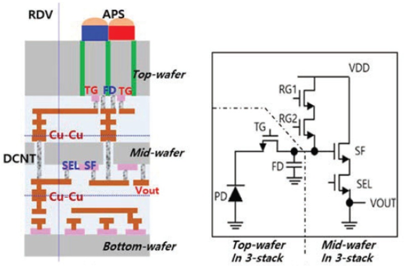
Schematic of a three-layer stacked CIS architecture featuring in-pixel Copper-to-Copper (Cu-Cu) bonding. Adapted from Ref. [21].
3.4 Advanced Pixel Transistors
Innovations at the fundamental transistor level are a cornerstone of modern noise reduction efforts, directly targeting the physical origins of thermal, flicker, and RTS noise. Several techniques are employed:
1) Gate Oxide (GOX) Engineering: GOX engineering plays a critical role in mitigating noise in scaled CMOS image sensor pixels through various structural and process-level optimizations [24]. A primary strategy is to thin the SF gate oxide to increase gate capacitance (Cox), which is inversely proportional to the amplitude of RTS noise. For instance, in a 0.64 μm pixel design, thinning the GOX accounted for approximately 50% of the total observed RTS improvement [25]. Beyond physical scaling, the choice of oxidation technique significantly influences the noise characteristics of narrow-channel SFs. Benchmarking results indicate that Furnace and Rapid Thermal Oxidation (RTO) provide superior noise performance compared to Nitridation processes, as the latter can degrade interface quality or increase the effective oxide thickness (EOT), thereby elevating noise populations. To further enhance interface uniformity and passivation, advanced treatments such as Low-Pressure Radical Oxidation (LPRO) and UV curing have been explored, demonstrating modest reductions in blinking pixels (Fig. 4(a)) [26]. Furthermore, chemical passivation via fluorine implantation has been shown to be effective at neutralizing Si-SiO2 interface traps, as shown in Fig. 4(b) [27]. By optimizing the implantation dose and sequence—specifically by performing the implant after nitride spacer formation to act as a diffusion barrier—fluorine is effectively retained within the oxide. This optimized method achieved a 14% reduction in RTS noise while successfully avoiding the bubble defects typically associated with excessive fluorine doses [27].
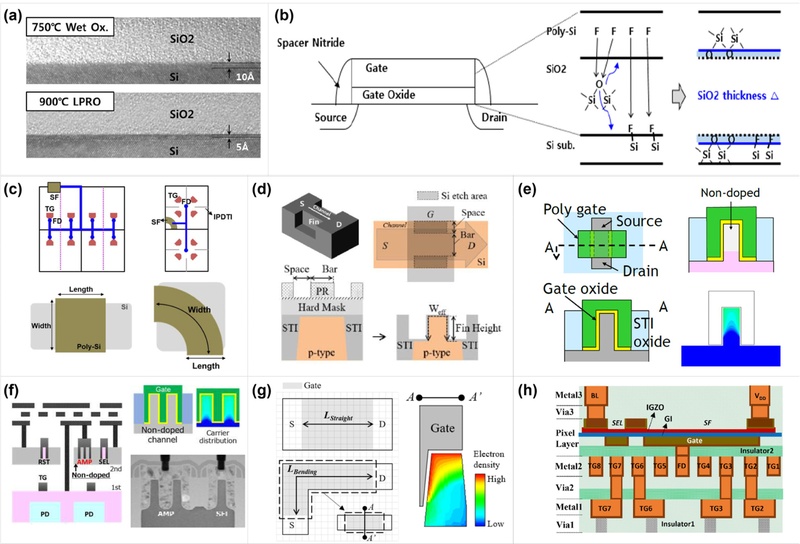
Transistor-level innovations for temporal noise reduction. (a) LPRO/UV gate oxide treatments and (b) Fluorine passivation for interface trap neutralization. Adapted from Ref. [26] and [27]. (c) Quarter-Ring (QR) layout for 20% gm enhancement. Adapted from Ref. [28]. (d) Pixel-FinFET and (e) Buried Gate using Si(100) sidewalls to minimize Dit. Adapted from Ref. [29] and [22]. (f) 2-Fin structure for 99.3% RTS reduction. Adapted from Ref. [23]. (g) 3D Bending SF for ultra-small pixel pitch. Adapted from Ref. [30]. (h) Monolithic BEOL IGZO transistor integration. Adapted from Ref. [31].
2) Novel Layout Design: To address the transconductance (gm) degradation caused by the limited active area in sub-micron pixels incorporating Front-Side Deep-Trench Isolation (FDTI), a novel Quarter-Ring (QR) source follower with an asymmetric drain-to-source layout has been proposed as shown in Fig. 4(c) [28]. By implementing a radial current path that maximizes the utilization of the confined corner spaces surrounding the FDTI, the QR SF architecture effectively achieves a 20% enhancement in both fill factor and gm compared to conventional rectangular layouts. Consequently, this geometric optimization leads to a significant reduction in temporal read noise, attaining a sub-electron noise floor of 0.98 and a high dynamic range of 86.2 dB in a 1.28 μm 50-megapixel CMOS image sensor.
3) 3D Multi-gate Pixel Transistors: To overcome the area constraints of conventional planar transistors, Multi-Gate Pixel Transistors have been introduced to increase effective channel width (Weff) and transconductance (gm). Pixel-FinFETs represent a direct adaptation of FinFET technology tailored for the analog requirements of image sensors, focusing on maximizing the channel perimeter within a single lithography step (Fig. 4(d)) [29]. Unlike logic FinFETs, which require complex multi-patterning for high density, Pixel-FinFETs are fabricated using a cost-effective single-step photolithography followed by silicon dry etching. This process allows for flexible fin-height tuning. A Pixel-FinFET with optimized fin height demonstrated a 37% increase in gm compared to planar counterparts, translating to an 88% increase in Weff. Consequently, the sub-threshold swing improved from 100 mV/dec to 65 mV/dec, indicating superior channel control. In wafer-level testing, the population of pixels exhibiting significant RTS noise dropped from 100% in planar references to just 32.4%.
In stacked pixel structures, Pixel-FinFETs are often implemented using a “buried gate” architecture formed by the full-etching of the Shallow Trench Isolation (STI) as illustrated in Fig. 4(e) [22]. This device is customized for CIS using a highly controllable STI full-etching process that exposes the silicon sidewalls, effectively wrapping the gate around the channel to maximize Weff without increasing the footprint. A critical innovation in this architecture is the optimization of sidewall crystal orientation; while planar devices typically utilize the Si(110) plane, the multi-gate structure is designed to expose the Si(100) plane on the fin sidewalls. Si(100) has a lower interface-state density (Dit) than Si(110), thereby reducing 1/f noise components. Furthermore, the 2-layer stacked structure physically isolates the SF from the PD, enabling the use of a completely non-doped channel. This moves the carrier flow path away from the Si/SiO2 interface traps and impurity scattering centers. Compared to a planar transistor of the same footprint, this multi-gate transistor achieved a 43% improvement in gm and a 91% reduction in RTS noise. Additionally, the buried gate structure minimizes total gate capacitance (Cgg), helping to maintain high conversion gain. The 2-layer architecture further facilitates the integration of larger, high-performance devices, such as 2-Fin FinFETs, as shown in Fig. 4(f) [23]. Doubling the Weff through a 2-Fin structure resulted in a 2.42-fold improvement in gm and a remarkable 99.3% reduction in RTS noise compared to the planar SF reference (from 1,983 ppm to 13 ppm), effectively eliminating RTS as a dominant noise source in sub-micron pixels.
In ultra-small pixels (e.g., 0.5 μm pitch), layout constraints often force the SF transistor into an L-shaped or bent geometry. Recent research has integrated 3D vertical gates into these bending structures using the 3D Bending Source Follower (3D-SF), which is formed by recessing the field oxide near the channel region, as shown in Fig. 4(g) [30]. Research indicates that the vertical gate depth is a critical parameter; increasing this depth from 0.63 × W to 0.88 × W (where W is the planar width) significantly enhances performance. The optimized 3D bending structure improves gm by approximately 9% and Weff by 20% compared to a planar bending SF. This geometric expansion results in a 62% reduction in wafer-level RTS noise and a 7% reduction in total temporal noise, proving that 3D vertical integration is effective even in non-linear layout topologies.
4) Back-End-of-Line (BEOL) IGZO Transistors: Huawei has pioneered a monolithic dual-layer pixel design that integrates Indium-Gallium-Zinc-Oxide (IGZO) transistors directly into the back-end-of-line (BEOL) metal layers above the silicon PD, a process made possible by IGZO's low thermal budget (<400°C), which is compatible with front-end CMOS devices (Fig. 4(h)) [31]. This approach offers several distinct advantages for noise performance: 1) The input-referred noise voltage (SVg) is comparable in magnitude to that of conventional silicon transistors. 2) The transistors achieve a low RMS voltage noise (VRMS) of under 100 μV, even for highly scaled gate lengths (Lg = 65 nm). 3) They exhibit exceptional stability under Positive Bias Temperature Instability (PBTI) and HCI stress, ensuring reliable and consistent low-noise operation over the sensor's lifetime.
3.5 Readout Techniques for Temporal Noise Suppression
To minimize input-referred temporal noise in sub-micron CMOS image sensors, various signal-processing and readout strategies have been implemented to mitigate the trade-off between noise performance and readout speed. Conditional Correlated Multiple Sampling (CCMS) represents a significant advancement over conventional CDS by applying multiple sampling iterations exclusively to small-swing signals using a small-range voltage ramp, thereby achieving a read noise of 0.66 while mitigating the frame rate degradation typically associated with full-range multi-sampling [32]. Similarly, oversampling-based noise reduction techniques, which optimize the balance between ADC bit-depth and sampling frequency (e.g., 10-bit resolution with 4 × oversampling), have demonstrated the capability to lower read noise to 0.55 when combined with high analog gain [12]. In the domain of pixel-level ADCs, the Noise-Bandwidth Limiting (nBWL) technique utilizes a dedicated in-pixel capacitor (e.g., 100 fF) to reduce the operational transconductance amplifier's -3dB cutoff frequency, effectively filtering out high-frequency thermal noise by over 30% [33]. Furthermore, architectural innovations such as parallel multiple sampling using double column ADCs allow for the averaging of uncorrelated noise components to achieve a 3dB improvement [34], while the Reset-Signal-Signal (RSS) readout sequence in dual-pixel sensors prevents the noise penalty inherent to separate A/D conversions by performing charge-domain summation without an intermediate reset [35].
3.6 Photon-Counting CMOS image sensors
The Quanta Image Sensor (QIS) represents a paradigm shift in imaging technology by enabling deterministic single-electron photon counting. Unlike conventional CIS, which integrates a large number of photoelectrons into an analog signal, the QIS uses an ensemble of specialized sub-diffraction pixels called “jots”. These jots are designed with ultra-high conversion gain and deep sub-electron read noise—specifically targeting a noise floor below 0.15 —to ensure a sufficiently low probability of error during the quantization of individual charge carriers. For instance, Fig. 5(a) presents an image captured under ultra-low-light conditions using a 16.7 MP QIS featuring a 1.1 μm pixel pitch and a deep sub-electron read noise of 0.19 [36].
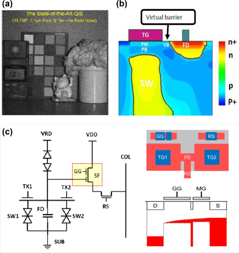
Performance and architectures of high-resolution QIS. (a) Ultra-low-light image from a QIS. Adapted from Ref. [36]. (b) Pump Gate (PG) schematic with distal FD and zero overlap for parasitic capacitance reduction. Adapted from Ref. [36]. (c) MGSF utilizing decoupled gates for 1/f noise suppression and high CG (716 μV/e−). Adapted from Ref. [38].
Operating on the principles of spatial and temporal oversampling, the QIS captures a massive sequence of binary or multi-bit bit planes at high frame rates. These snapshots are subsequently processed using digital bit summation to reconstruct a high-dynamic-range image. By shifting the complexity from the analog domain to the digital domain, the QIS effectively circumvents the fundamental trade-offs between read noise, full-well capacity, and dynamic range inherent in traditional integration-based sensors.
Recent advancements in QIS technology have achieved deep sub-electron read noise, even in sub-micron pixel architectures. A pivotal development is the implementation of the Pump Gate (PG) pixel design as shown in Fig. 5(b) [36], which features a distal FD with zero overlap between the transfer gate and the FD to minimize parasitic capacitance [37]. This structure has demonstrated a median input-referred read noise of 0.8 in 0.8 μm pixels, significantly outperforming conventional pinned PD designs. Furthermore, it effectively eliminates hot pixels by increasing the separation between the PD and the silicon interface. State-of-the-art QIS devices have further pushed these boundaries, achieving a read noise of 0.19 and a high CG of 340 μV/e−, enabling the direct observation of dark signal quantization and discrete electron counting [36].
To overcome the scaling trade-off between 1/f noise and conversion gain, the Multi-Gate Source-Follower (MGSF) architecture has been introduced as shown in Fig. 5(c) [38]. This design utilizes separate modulation and guard gates to simultaneously maximize the effective gate area for noise suppression and minimize input capacitance for high CG. Simulation results indicate that MGSF configurations can enhance the FD-referred CG by approximately 20%, reaching 716 μV/e−, while significantly mitigating 1/f noise relative to baseline transistors. Complementary research into 1/f noise modeling has validated that buried-channel source followers and mobility-fluctuation-based models accurately predict noise behavior. This enables further optimization through cryogenic operation, where read noise can be reduced to 0.18 at -70°C [39].
3.7 Future perspectives
Table 1 provides a comprehensive performance comparison of CIS incorporating the latest advancements in noise–reduction technology. Looking forward, the increasing demand for Wide Dynamic Range (WDR) has further prioritized the suppression of low-light noise. As pixel pitches continue to scale into the deep sub-micron regime, the industry is expected to accelerate the transition toward 3D gate structures and stacked transistor architectures, mirroring the structural evolution observed in leading-edge logic nodes such as FinFET, Gate-all-around FET, and Complementary FET. In this context, IGZO TFTs integrated on the BEOL layer are emerging as promising candidates for pixel-level transistors, offering ultra-low leakage paths that could further suppress dark-current-related noise components.

Comparative summary of key performance metrics for CMOS image sensors from major companies and institutes.
Furthermore, to overcome the fundamental trade-off between pixel scaling and CG, advanced interconnect technologies will undergo significant refinement, most notably through local poly-Si routing. By minimizing the parasitic capacitance associated with in-pixel wiring, these localized routing techniques will enable drastic reductions in node capacitance. Beyond hardware-centric optimizations, the paradigm of noise suppression is shifting toward on-device AI-driven denoising. Integrating lightweight neural networks directly into the sensor's readout circuitry or a companion image signal processor (ISP) will enable real-time removal of complex temporal and spatial noise.
4. CONCLUSION
This review summarizes the challenges and mitigation strategies for temporal noise in sub-micron mobile CMOS image sensors. To maintain SNR despite aggressive pixel scaling, recent technological advancements have converged on three synergistic strategies.
First, device-level breakthroughs have transitioned from planar structures to 3D topologies—such as Pixel-FinFETs and 3D bending SFs—while incorporating BEOL IGZO transistors to maximize effective channel area and device reliability. Second, pixel-level innovations, including multi-layer stacked architectures and high-CG designs such as Locally Lowered-Stack, have enabled the integration of larger SF transistors and improved input-referred noise. Third, advanced readout schemes, notably Noise-Bandwidth Limiting, have further enhanced signal integrity by filtering low-frequency noise.
Looking forward, the future of low-light imaging lies in deterministic photon counting. Technologies like QIS with deep sub-electron read noise, combined with emerging on-device AI denoising, are poised to push mobile imaging performance toward the ultimate physical limit of single-photon sensitivity.
Acknowledgments
This work was supported by the Academic Promotion System of the Tech University of Korea.
REFERENCES
-
A. Boukhayma, A. Peizerat, C. Enz, Noise Reduction Techniques and Scaling Effects towards Photon Counting CMOS Image Sensors, Sensors 16 (2016) 514.
[https://doi.org/10.3390/s16040514]

-
M.K. Rai, S. Rai, Low-frequency noise characterization and thermal stability analysis of negative capacitance junction-less transistors, Integr. Ferroelectr. 232 (2023) 43–62.
[https://doi.org/10.1080/10584587.2023.2173441]
- 3D Random Telegraph Noise Simulator for Development of High-Resolution CMOS Image Sensor. https://www.global.toshiba/ww/technology/corporate/rdc/rd/fields/12-e12.html, , 2026 (accessed 11 March 2026).
- X. Wang, Noise in sub-micron CMOS image sensors, Ph.D. thesis, TU Delft, Delft, Netherlands, 3rd November 2008.
- C.Y.-P. Chao, M.-H. Wu, S.-F. Yeh, C.-L. Lee, C. Yin, K.-Y. Chou, et al., Characterization of Random Telegraph Noises of MOSFET Subthreshold Currents for a 40 nm Process, Proceedings of the 2021 International Image Sensor Workshop (IISW), Online (Virtual Event), 2021, p. R10.
- C.Y.-P. Chao, M.-H. Wu, S.-F. Yeh, K.-Y. Chou, H. Tu, C.-L. Lee, et al., Identifying the Sources of Random Telegraph Noises in Pixels of CMOS Image Sensors, Proceedings of 2019 the International Image Sensor Workshop (IISW), Snowbird, UT, USA, 2019, p. R10.
- C.Y.-P. Chao, M.-H. Wu, S.-F. Yeh, C.-L. Lee, C. Yin, H. Tu, Hot Carrier Injection Induced Random Telegraph Noise Degradation in a 0.8 μm-pitch 8.3Mpixel Stacked CMOS Image Sensor, Proceedings of the 2023 International Image Sensor Workshop (IISW), Crieff, Scotland, UK, 2023, p. R2.
- C. Chao, T. Wu, C. Liu, S.-F. Yeh, C.-L. Lee, H. Tu, et al., Recovery of Random Telegraph Noises in a Stacked CMOS Image Sensor by High-Temperature Annealing after Hot-Carrier Stress, Proceedings of the 2025 International Image Sensor Workshop (IISW), Awaji, Hyogo, Japan, 2025, p. R03.2.
- S.-F. Yeh, M.-H. Wu, C.-L. Lee, C. Yin, K.-Y. Chou, C.Y.-P. Chao, Random Telegraph Noise Caused by MOSFET Channel Traps and Variable Gate Induced Leakage with Multiple Sampling Readout, Proceedings of the 2019 International Image Sensor Workshop (IISW), Snowbird, UT, USA, 2019, p. R12.
- A. Antonsanti, J.-M. Lauenstein, A.L. Roch, L. Ryder, C. Virmontois, V. Goiffon, Exploring Space-Radiation Induced Dark Signal and Random-Telegraph-Signal in a Sony IMX219 CMOS Image-Sensor, Proceedings of the 2023 International Image Sensor Workshop (IISW), Crieff, Scotland, UK, 2023, p. R23.
- P. Centen, The source-to-gate capacitance of the in-pixel source follower: a positive feedback during charge sensing which increases column settling time and noise voltage, Proceedings of the 2023 International Image Sensor Workshop (IISW), Crieff, Scotland, UK, 2023, p. R35.
-
M.-S. Keel, K.-M. Kim, H. Seo, S.-Y. Park, M. Lee, D. Kim, et al., A 12-Mpixel Automotive Image Sensor with 137-dB Single-Exposure Dynamic Range and 0.55-Electron Read Noise by Oversampling-Based Noise Reduction, Proceedings of the 2025 Symposium on VLSI Technology and Circuits, Kyoto, Japan, 2025, pp. 1–3.
[https://doi.org/10.23919/VLSITechnologyandCir65189.2025.11074844]
-
M.-W. Seo, Y.-S. Choi, S. Lee, M. Ito, D. Bae, Y. Shim, et al., A 1.22 E-Rms Temporal Random Noise, 110 dB High Dynamic Range, 2.988 μm Pixel-pitch 3-Stacked Digital Pixel Sensor With on-Chip HDR Merger, Proceedings of the 2025 Symposium on VLSI Technology and Circuits, Kyoto, Japan, 2025, pp. 1–3.
[https://doi.org/10.23919/VLSITechnologyandCir65189.2025.11074898]
-
S. Lee, J. Cho, S. Choi, S.Y. Min, E. Lee, M. Jung, et al., A Temporal Noise Reduction via 40% Enhanced Conversion Gain in Dual-Pixel CMOS Image Sensor with Full-Depth Deep-Trench Isolation and Locally Lowered-Stack Technology, Proceedings of the 2024 IEEE Symposium on VLSI Technology and Circuits, Honolulu, HI, USA, 2024, pp. 1–2.
[https://doi.org/10.1109/VLSITechnologyandCir46783.2024.10631436]
-
D. Kim, K. Cho, H.-C. Ji, M. Kim, J. Kim, T. Kim, et al., A 1/1.56-inch 50Mpixel CMOS Image Sensor with 0.5 μm pitch Quad Photodiode Separated by Front Deep Trench Isolation, Proceedings of the 2024 IEEE International Solid-State Circuits Conference (ISSCC), San Francisco, CA, USA, 2024, pp. 118–120.
[https://doi.org/10.1109/ISSCC49657.2024.10454448]
-
Y. Satake, Y. Tanaka, S. Sato, M. Takase, M. Hoyano, S. Kasukawa, et al., Low Dark Noise and 8.5k e- Full Well Capacity in a 2-Layer Transistor Stacked 0.8 μm Dual Pixel CIS with Intermediate Poly-Si Wiring, Proceedings of the 2024 IEEE International Electron Devices Meeting (IEDM), San Francisco, CA, USA, 2024, pp. 1–4.
[https://doi.org/10.1109/IEDM50854.2024.10873371]
- M. Sugimoto, T. Okawa, K. Suzuki, T. Ogita, K. Nishida, K. Hiramatsu, T. Hirano, et al., High full well capacity and low noise characteristics in 0.6 μm pixels via buried sublocal connections in a 2-layer transistor pixel stacked CMOS image sensor, Proceedings of the 2023 International Image Sensor Workshop (IISW), Crieff, Scotland, UK, 2023, p. R12.
- G. Park, J. Song, K. Cho, S. Kim, Y. Park, Y. Kim, et al., Improvement of Conversion Gain and Pixel Linearity through Source Follower Drain Design in CMOS image sensors, Proceedings of the 2025 International Image Sensor Workshop (IISW), Hyogo, Japan, 2025, p. P04.
- M. Kim, D. Kim, K. Chang, K. Woo, K. Yoon, H. Ko, et al., A 0.5 μm pixel-pitch 200-Megapixel CMOS Image Sensor with Partially Removed Front Deep Trench Isolation for Enhanced Noise Performance and Sensitivity, Proceedings of the 2025 International Image Sensor Workshop (IISW), Hyogo, Japan, 2025, p. R01.2.
-
S.-S. Kim, G.-D.R. Lee, S.-S. Park, H. Shim, D.-H. Kim, M. Choi, et al., 3-Layer Stacked Voltage-Domain Global Shutter CMOS Image Sensor with 1.8 μm-Pixel-Pitch, Proceedings of the 2022 International Electron Devices Meeting (IEDM), San Francisco, CA, USA, 2022, pp. 37.5.1–37.5.4.
[https://doi.org/10.1109/IEDM45625.2022.10019515]
-
G.-D.R. Lee, D.-H. Kim, D. Kwon, J.-E. Park, D. Cho, J. Kang, et al., A 0.5 µm Pixel 3-layer Stacked CMOS Image Sensor with Deep Contact and In-pixel Cu-Cu Bonding Technology, Proceedings of the 2023 International Electron Devices Meeting (IEDM), San Francisco, CA, USA, 2023, pp. 1–4.
[https://doi.org/10.1109/IEDM45741.2023.10413687]
-
S. Kitamura, N. Kimizuka, A. Honjo, K. Baba, T. Kurobe, H. Kumano, et al., Low-Noise Multi-Gate Pixel Transistor for Sub-Micron Pixel CMOS Image Sensors, Proceedings of the 2022 IEEE Symposium on VLSI Technology and Circuits, Honolulu, HI, USA, 2022, pp. 347–348.
[https://doi.org/10.1109/VLSITechnologyandCir46769.2022.9830386]
-
Y. Kikuchi, M. Tomita, T. Hayashi, H. Chiba, T. Ogita, T. Okawa, et al., Noise Performance Improvements of 2-Layer Transistor Pixel Stacked CMOS Image Sensor with Non-doped Pixel-FinFETs, Proceedings of the 2023 Symposium on VLSI Technology and Circuits, Kyoto, Japan, 2023, pp. 1–2.
[https://doi.org/10.23919/VLSITechnologyandCir57934.2023.10185422]
- M.G.Da Cunha, S. Place, O. Gourhant, S. Haendler, P. Magnan, P. Martin-Gonthier, et al., Gate Oxide Benchmarking for Low Frequency Noise Improvement On 3D Stacked CMOS Image Sensors, Proceedings of the International Image Sensor Workshop (IISW), Crieff, Scotland, UK, 2023, pp. 1–4.
-
J. Park, S. Park, K. Cho, T. Lee, C. Lee, D. Kim, et al., 1/2.74-inch 32Mpixel-Prototype CMOS Image Sensor with 0.64 μm Unit Pixels Separated by Full-Depth Deep-Trench Isolation, Proceedings of the 2021 IEEE International Solid-State Circuits Conference (ISSCC), San Francisco, CA, USA, 2021, pp. 122–124.
[https://doi.org/10.1109/ISSCC42613.2021.9365751]
- M. Ha, D. Oh, S. Park, W. Choi, H. Lee, B. Lee, et al., Several Process Techniques & Pixel Source Follower Schemes to improve the Pixel Temporal Noise, Proceedings of the International Image Sensor Workshop (IISW), Snowbird, UT, USA, 2019, p. R08.
- S. You, J. Lee, D. Im, S. Choi, T. Lee, S. Lee, et al., Reduction of RTS noise by optimizing fluorine implantation in CMOS image sensor, Proceedings of the International Image Sensor Workshop (IISW), Crieff, Scotland, UK, 2023, P. R25.
-
H. Kim, Y.H. Kim, S. Moon, H. Kim, B. Yoo, J. Park, et al., A 0.64 μm 4-Photodiode 1.28 μm 50Mpixel CMOS Image Sensor with 0.98e- Temporal Noise and 20Ke- Full-Well Capacity Employing Quarter-Ring Source-Follower, Proceedings of the 2023 IEEE International Solid-State Circuits Conference (ISSCC), San Francisco, CA, USA, 2023, pp. 96–98.
[https://doi.org/10.1109/ISSCC42615.2023.10067732]
- S. Kim, D. Kim, C.K. Chang, K. Oh, S. Kim, K. Lee, et al., Low-noise and High-performance 3-D Pixel Transistor for Sub-micron CMOS Image Sensors Applications, Proceedings of the International Image Sensor Workshop (IISW), Online (Virtual Event), 2021, pp. 1–4.
- K.E. Chang, D. Im, S. Kim, D. Kim, J. Go, I. Cho, et al., Low-noise 3-D Bending Pixel Transistor for Small Pixel CMOS Image Sensors, Proceedings of the International Image Sensor Workshop (IISW), Crieff, Scotland, UK, 2023, p. R32.
-
S. Zhan, K. Kaneko, H. Wang, L. Kang, Y. Li, W. Cui, et al., A Monolithic Dual-Layer Pixel Design with BEOL IGZO Transistors Featuring High Dual Conversion Gain Ratio and Scaled Pixel Size for Future Image Sensors, Proceedings of the 2025 Symposium on VLSI Technology and Circuits, Kyoto, Japan, 2025, pp. 1–3.
[https://doi.org/10.23919/VLSITechnologyandCir65189.2025.11074832]
- S.-F. Yeh, K.-Y. Chou, H.-Y. Tu, C.Y.-P. Chao, f.-L. Hsueh, A 0.66 e-rms temporal-readout-noise 3D-stacked CMOS image sensor with conditional correlated multiple sampling (CCMS) technique, Proceedings of the 2015 Symposium on VLSI Technology and Circuits, Kyoto, Japan, 2015, pp. C84–C85.
- S. Lee, M.-W. Seo, M. Ito, S.-J. Byun, H. Kwon, D. Bae, et al., Temporal Noise Suppression Method using Noise-Bandwidth Limitation for Pixel-Level Single-Slope ADC, Proceedings of the International Image Sensor Workshop (IISW), Crieff, Scotland, UK, 2023, pp.1–4.
-
A. Suzuki, N. Shimamura, T. Kainuma, N. Kawazu, C. Okada, T. Oka, et al., A 1/1.7-inch 20Mpixel Back-illuminated stacked CMOS image sensor for new imaging applications, Proceedings of the IEEE International Solid-State Circuits Conference (ISSCC), San Francisco, CA, USA, 2015, pp. 1–3.
[https://doi.org/10.1109/ISSCC.2015.7062950]
- J. Yun, K. Lee, J. Pyo, K. Lee, S. Lee, M. Fujita, et al., A Small-size Dual Pixel CMOS Image Sensor with Vertically Broad Photodiode of 0.61 μm pitch, Proceedings of the International Image Sensor Workshop (IISW), Snowbird, UT, USA, 2019, p. R03.
- J. Krynski, D. McGrath, A.L. Roch, S. Holloway, L. Migliorin, V. Lalucaa, et al., Dark Signal Quantization and Random Telegraph Signal in a Quanta Image Sensor, Proceedings of the 2025 International Image Sensor Workshop (IISW), Hyogo, Japan, 2025, p. R03.3.
- L. Anzaigra, J. Ma, D. Hondongwa, D. Zhang, S. Masoodian, Performance Analysis of Two Low-Noise 0.8 µm Pixel Designs, Proceedings of the International Image Sensor Workshop (IISW), Online (Virtual Event), 2021, P. R06.
- W. Deng, E.R. Fossum, Multi-Gate Source-Follower for Quanta Image Sensors (QIS), Proceedings of the 2021 International Image Sensor Workshop (IISW), Online (Virtual Event), 2021, p. R09.
- W. Deng, D. Starkey, J. Ma, E.R. Fossum, Modelling Measured 1/f Noise in Quanta Image Sensors (QIS), Proceedings of the 2019 International Image Sensor Workshop (IISW), Snowbird, UT, USA, 2019, pp. R07.
- C.Y. Ai, K. Watanabe, S. Lee, G. Park, A. Imaizumi, K.W. Yeung, et al., 0.56 µm-pitch CMOS image sensor for high resolution application, Proceedings of the International Image Sensor Workshop (IISW), Crieff, Scotland, UK, 2023, pp. 22–25.
- W. Choi, M. Kim, J. Kim, J. Seok, Y. Song, D. Park, et al., A 9-shared 3x3 Nonacell Image Sensor with 0.64 μm unit pixels for Read Noise and Low-illuminance SNR enhancement, Proceedings of the International Image Sensor Workshop (IISW), Crieff, Scotland, UK, 2023.
- M. Uchiyama, G. Park, S. Lee, T. Tate, M. Minagawa, S. Shimoyamada, et al., A 40/22 nm 200MP stacked CMOS image sensor with 0.61 µm pixel, Proceedings of the International Image Sensor Workshop (IISW), Online (Virtual Event), 2021, P. R02.
-
Y. Kim, W. Choi, D. Park, H. Jeoung, B. Kim, Y. Oh, et al., A 1/2.8-inch 24Mpixel CMOS image sensor with 0.9 μm unit pixels separated by full-depth deep-trench isolation, Proceedings of the 2018 IEEE International Solid-State Circuits Conference (ISSCC), San Francisco, CA, USA, 2018, pp. 84–86.
[https://doi.org/10.1109/ISSCC.2018.8310195]
- T. Hasegawa, K. Watanabe, Y.J. Jung, N. Tanaka, T. Nakashikiryo, W.-Z. Yang, et al., A new 0.8 µm CMOS image sensor with low RTS noise and high full well capacity, Proceedings of the International Image Sensor Workshop (IISW), Snowbird, UT, USA, 2019, p. R02.
-
K. Zaitsu, A. Matsumoto, M. Nishida, Y. Tanaka, H. Yamashita, Y. Satake, et al., A 2-Layer Trans is tor Pixel Stacked CMOS Image Sensor with Oxide-Based Full Trench Isolation for Large Full Well Capacity and High Quantum Efficiency, Proceedings of the 2022 IEEE Symposium on VLSI Technology and Circuits, Honolulu, HI, USA, 2022, pp. 286–287.
[https://doi.org/10.1109/VLSITechnologyandCir46769.2022.9830372]
-
V.C. Venezia, A.C.-W. Hsiung, K. Ai, X. Zhao, Z. Lin, D. Mao, et al., 1.5 µm Dual Convers ion Gain, Backs ide Illuminated Image Sensor Using Stacked Pixel Level Connections with 13ke- Full-Well Capacitance and 0.8e-Noise, Proceedings of the 2018 IEEE International Electron Devices Meeting (IEDM), San Francisco, CA, USA, 2018, pp. 10.1.1–10.1.4.
[https://doi.org/10.1109/IEDM.2018.8614484]
- S. Baek, S. An, D. Sul, M. Fujita, S. Jung, Y. Na, et al., A 0.45 µm-pitch Photodiode Based 1-layer Dual Pixel for CMOS Image Sensor with High Full-Well Capacity and Low Noise, Proceedings of the International Image Sensor Workshop (IISW), Hyogo, Japan, 2025, p. R01.3.
-
S. Park, C. Lee, S. Park, H. Park, T. Lee, D. Park, et al., A 64Mpixel CMOS Image Sensor with 0.56 μm Unit Pixels Separated by Front Deep-Trench Isolation, Proceedings of the 2022 IEEE International Solid-State Circuits Conference (ISSCC), San Francisco, CA, USA, 2022, pp. 108–110.
[https://doi.org/10.1109/ISSCC42614.2022.9731750]
- S. Choi, S. Lee, T. Lee, H. Ji, H. Park, D. Im, et al., World smallest 200Mp CMOS Image Sensor with 0.56 μm pixel equipped with novel Deep Trench Isolation structure for better sensitivity and higher CG, Proceedings of the International Image Sensor Workshop (IISW), Crieff, Scotland, UK, 2023, p. R13.
-
Y.J. Jung, V.C. Venezia, S. Lee, C.Y. Ai, Y. Zhu, K.W. Yeung, et al., A 64M CMOS Image Sensor using 0.7 μm pixel with high FWC and switchable conversion gain, Proceedings of the 2020 IEEE International Electron Devices Meeting (IEDM), San Francisco, CA, USA, 2020, pp. 16.3.1–16.3.4.
[https://doi.org/10.1109/IEDM13553.2020.9371889]
-
M. Sato, Y. Yorikado, Y. Matsumura, H. Naganuma, E. Kato, T. Toyofuku, et al., A 0.50-rms Noise 1.45 µm-Pitch CMOS Image Sensor with Reference-Shared In-Pixel Differential Amplifier at 8.3Mpixel 35fps, Proceedings of the 2020 IEEE International Solid-State Circuits Conference (ISSCC), San Francisco, CA, USA, 2020, pp. 108–110.
[https://doi.org/10.1109/ISSCC19947.2020.9063017]
-
T. Nishihara, M. Matsumura, T. Imoto, K. Okumura, Y. Sakano, Y. Yorikado, et al., An experimental CMOS photon detector with 0.5 e-RMS temporal noise and 15 μm pitch active sensor pixels, Proceedings of the 2017 IEEE International Electron Devices Meeting (IEDM), San Francisco, CA, USA, 2017, pp. 16.1.1–16.1.4.
[https://doi.org/10.1109/IEDM.2017.8268400]
-
H. Kim, J. Park, I. Joe, D. Kwon, J.H. Kim, D. Cho, et al., A 1/2.65in 44Mpixel CMOS Image Sensor with 0.7 µm Pixels Fabricated in Advanced Full-Depth Deep-Trench Isolation Technology, Proceedings of the 2020 IEEE International Solid-State Circuits Conference (ISSCC), San Francisco, CA, USA, 2020, pp. 104–106.
[https://doi.org/10.1109/ISSCC19947.2020.9062924]

Incheol Cho is an Assistant Professor in the Department of Advanced Materials Engineering at Tech University of Korea (TU Korea). He received his B.S., M.S., and Ph.D. in Mechanical Engineering from KAIST in 2015, 2017, and 2021, respectively. Previously, he served as a staff engineer at the Semiconductor R&D Center of Samsung Electronics, where he contributed to the development of 0.5 μm-pitch ultra-fine pixels and low-noise transistors. His current research interests focus on micro/nano technology-based environmental sensors, next-generation image sensors, and AI-converged sensor technologies.