
Development of a Foam-Based Nanopatterning Method for Fabricating High-Aspect-Ratio Polymeric Nanowires
ⓒ The Korean Sensors Society
This is an Open Access article distributed under the terms of the Creative Commons Attribution Non-Commercial License (https://creativecommons.org/licenses/by-nc/3.0/) which permits unrestricted non-commercial use, distribution, and reproduction in any medium, provided the original work is properly cited.
Abstract
High-aspect-ratio polymeric nanowires are promising structural elements for sensor development because they provide large interfacial areas, continuous transport pathways, and mechanical compatibility with soft or flexible substrates. However, simple and scalable fabrication of long, narrow, and well-aligned polymeric nanowire patterns remains challenging. Here, we present a foam-based nanopatterning method using a flexible through-hole film as a template for generating well-ordered two-dimensional foams. During solvent evaporation of the foam, motion of liquid-air interface guides solutions into narrow line-shaped regions between the device and substrate. Device geometry was optimized through experimental observation and numerical analysis to promote stable meniscus confinement and continuous line formation. Using 500 nm-diameter polystyrene particles, the optimized device generated single-particle-wide polymeric nanowire patterns with a width of approximately 500 nm and a length of approximately 300 µm. Reactive ion etching was further explored to reduce the nanowire width after patterning. This approach offers a simple and lithography-light route for fabricating polymeric nanowire patterns potentially useful for flexible, optical, chemical, and biological sensor interfaces.
Keywords:
Nanowires, Foam-based nanopatterning, High aspect ratio1. INTRODUCTION
Nanowire structures have attracted considerable attention as functional building blocks for sensor platforms. Because their nanoscale dimensions and high-aspect-ratio geometries provide large surface-to-volume ratios, enhanced interactions between analytes and sensors, and efficient signal transduction pathways [1-3]. Patterned nanowire arrays are particularly useful for sensors because they can increase the effective sensing interface, guide directional charge, ion, optical, or molecular transport, and confine electrical, chemical, or biological interactions within one-dimensional nanoscale geometries [4]. These features contribute to improved sensitivity, faster response, lower detection limits, and miniaturized device architectures. In addition, long and well-aligned nanowire patterns can establish continuous sensing pathways across extended device areas, which is important for flexible, wearable [5], optical [6], chemical [7,8], and biological sensing systems [9]. Among various material systems, polymeric nanowires are especially attractive because they provide mechanical flexibility, chemical tunability, low-cost processability, and compatibility with large-area or soft substrates. These advantages make them promising for deformable and bio-interfacing sensor platforms [10-12].
The ability to precisely control the width, length, alignment, and spatial arrangement of nanowires is essential for translating their intrinsic nanoscale properties into practical device-level functions [13]. Beyond nanoscale width control, increasing the length of nanowire patterns is also important, as long nanowires can provide continuous one-dimensional pathways across large device areas. Such extended pathways are advantageous; 1) maintaining electrical connectivity in flexible or stretchable electronics [14,15], 2) guiding anisotropic optical or photonic signals [16,17], 3) promoting directional molecular or ionic transport in sensing and filtration systems [18], 4) and increasing the interfacial contact area between the nanowire structure and the surrounding environment [19,20]. Therefore, long and narrow nanowire patterns can enhance device-level performance not only by providing nanoscale confinement but also by bridging nanoscale features with macroscopic functional architectures. However, fabricating long, narrow, and well-aligned polymeric nanowire patterns with high aspect ratios remains challenging, particularly when the process must be simple, scalable, and compatible with non-planar or flexible substrates.
Here, we present a foam-based nanopatterning strategy that uses a flexible through-hole film as a deformable template to generate high-aspect-ratio polymeric nanowire patterns. The central concept of this method is to exploit evaporation-induced meniscus motion and prevent surface-tension-driven deformation of the device, thereby stably guiding polymer assembly into long and narrow line patterns. The foam-based patterning has been previously demonstrated; however, parameter studies and approaches for increasing the aspect ratio of the resulting nanowire patterns have not been explored [21,22]. We describe the device structure and establish the working mechanism of foam-based nanopatterning. We show how the device geometry influences pattern formation through both experiments and numerical analysis. We further demonstrate the capability of this method by forming single-line polymeric nanowires, including single-particle-wide patterns composed of 500 nm-diameter polymer particles. As an additional route to enhance the aspect ratio, we examine reactive ion etching as a post-treatment process to reduce the patterned nanowire width. By enabling long-range, well-aligned polymeric nanowire structures without relying on conventional high-resolution lithography, this approach may broaden the practical use of polymer nanowire patterns in flexible electronics, optical and photonic devices, sensing interfaces, filtration systems, and bio-interface devices.
2. EXPERIMENTAL
2.1 Reagents and materials
All chemical reagents used in this study were obtained from Sigma-Aldrich unless specified otherwise. Negative-tone photoresists, including SU-8 3035 from Kayaku Advanced Materials, were employed for mold fabrication. Polydimethylsiloxane (PDMS; Sylgard 184, Dow Corning) and off-stoichiometry thiol–ene polymer resin (OSTEMER; OSTEMER 322 Crystal Clear, Mercene Labs) were used for the fabrication of a through-hole film with a post array. Polyvinyl alcohol (PVA; 360627) served as a sacrificial layer during film fabrication. The surfaces of the fabricated molds were treated with trichloro(1H,1H,2H,2H-perfluorooctyl)silane (PFOCTS; 448931) to facilitate demolding. For the preparation of a printing solution with 500 nm-diameter particles for printing nanowire patterns, sodium dodecyl sulfate (SDS; 436143) and 500 nm-diameter polystyrene particles (PSNPs; Fluoresbrite Carboxylate Microspheres, Polysciences) were dispersed in water. The PSNP suspension was diluted and used as received from the manufacturer, and the SDS concentration was adjusted to 0.05%.
2.2 Fabrication of devices for nanopatterning
The devices with through-hole and post arrays were fabricated based on a previously reported method [21,22]. Briefly, master molds were produced by forming two-layer SU-8 photoresist structures using standard photolithography. PDMS molds were then replicated from the master molds through conventional soft lithography and subsequently surface-functionalized with PFOCTS. A water-soluble sacrificial layer was prepared by spin-coating PVA onto a glass substrate, after which the PDMS mold was brought into conformal contact with the PVA-coated glass. Then, OSTEMER resin was introduced through the inlet port by negative pressure-driven flow. The loaded OSTEMER resin was initially cured by exposure to 365 nm UV light for 5 min. After curing, the PDMS mold was peeled off and could be reused. The patterned OSTEMER structure was further baked in an oven at 90 °C overnight to complete the solidification process. Finally, the device was released from the glass substrate by dissolving the PVA sacrificial layer in water.
3. RESULTS AND DISCUSSIONS
3.1 Device structure and working principle of foam-based nanopatterning
We first designed a flexible through-hole OSTEMER film as a mechanically deformable template for foam-based nanopatterning. The device was fabricated as a thin film containing periodically arranged circular through-holes and supporting posts. Owing to its flexible film structure, the device could be conformally attached to a target substrate and then removed after pattern formation (Fig. 1(a)). This conformal attachment is essential because the polymer-containing liquid must be confined within the narrow interface between the device and the substrate during evaporation. A photograph of the fabricated device shows a centimeter-scale through-hole film with an arrayed porous structure (Fig. 1(b)). Top-view microscopy confirmed the periodic arrangement of the through-holes and posts, while the cross-sectional image showed the thin-film geometry with characteristic lateral dimension of approximately 295 µm and 50 µm for through-hole and post, respectively (Fig. 1(c), (d)).
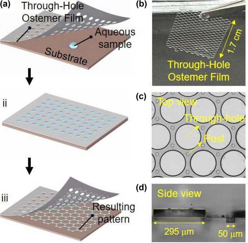
Structure of devices for foam-based nanopatterning (a) Schematic illustration showing the flexible nature of the device, which allows conformal attachment to a substrate. The gray region indicates the device, and the blue droplet represents the sample to be patterned. (b) Photograph of the device. (c) Top-view microscopy image of the device. (d) Cross-sectional microscopy image of the device.
The working principle of foam-based nanopatterning is illustrated in Fig. 2. After the device is placed on the substrate, a solution-processable material is introduced and confined at the film–substrate interface. In the initial state, the solution fills the region around the through-hole structures. As solvent evaporation proceeds, the air–liquid interface is generated around the through-holes and recedes, and the meniscus is progressively pinned at the post array. The time-dependent microscopy images show that the initially broad liquid-filled region evolves into narrower liquid bridges along the interstitial regions between neighboring posts. Finally, after complete evaporation, the polymeric material remains as line-shaped deposits following the confined meniscus pathways. Therefore, the final pattern is not directly defined by a nanoscale physical mold but is generated through the coupled effects of capillary confinement and evaporation-driven meniscus recession. This feature distinguishes foam-based nanopatterning from conventional lithographic patterning because the method uses evaporation and mechanical deformation to create nanoscale line patterns without requiring nanoscale channels, masks, or molds.
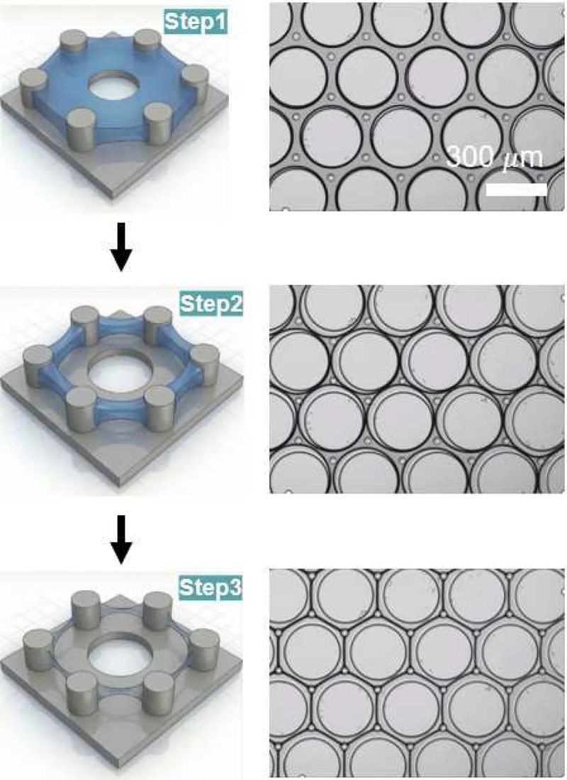
Working principle of foam-based nanopatterning using the device. The schematic illustrations show the device in a flipped orientation to better visualize the foam generation.
3.2 Optimization of device geometry for high-aspect-ratio nanowire patterning
Because the formation of narrow polymeric lines depends strongly on the deformation of the flexible through-hole film, we next investigated how the device geometry affects the patterning result. Fig. 3 compares two representative device designs and their corresponding patterning behaviors. In Design 1, the through-hole structure was surrounded by a relatively smaller area than the original design shown in Design 2. Although this geometry could generate polymeric deposits around the through-hole array, the resulting patterns were less uniform and less clearly confined. Moreover, attaching and preheating the through-hole template to improve conformal contact between its pillar array and the substrate led to more irregular deposited structures, likely due to deformation of the template roof during the annealing process.
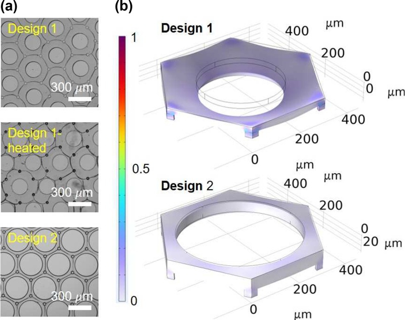
Design optimization of the device for patterning long and narrow nanowire structures on a substrate. (a) Top-view microscopy image of the patterns formed after foam-based nanopatterning with varied experimental conditions and device designs. (b) Numerical analysis of the mechanical response of the device under surface-tension-induced forces for the two designs. The color shows von Mises stress (N/m2).
In contrast, Design 2 produced more continuous and well-defined line patterns around the through-hole structures. The top-view microscopy image shows that the polymeric deposits were preferentially formed along the narrow interstitial regions between neighboring circular holes, resulting in a network-like arrangement of long line patterns. This improvement suggests that the geometry of Design 2 provides a more favorable balance between capillary confinement and mechanical deformation. In other words, the device should be sufficiently resistant to deformation to stably guide the liquid meniscus into narrow regions.
To understand this design-dependent behavior, numerical analysis was performed to compare the mechanical response of the two device geometries under surface-tension-induced loading. The simulation results show that Design 1 undergoes larger downward deformation near the through-hole region, whereas Design 2 exhibits a more restrained deformation profile (Fig. 3(b)). This difference is further quantified in Fig. 4 by performing the numerical simulation. The line-profile analysis indicates that the deformation in Design 1 increases steeply along the radial direction and reaches a much larger displacement than that in Design 2, due to the mechanically higher bending force applied by the surface tension. By contrast, Design 2 exphibits a relatively small, gradual displacement across the analyzed region. These results suggest that excessive deformation in Design 1 can cause a Laplace pressure difference between individually generated liquid-air interfaces, thereby resulting in irregular growth of foam. In contrast, the reduced deformation in Design 2 helps maintain a narrow and stable meniscus pathway during evaporation.
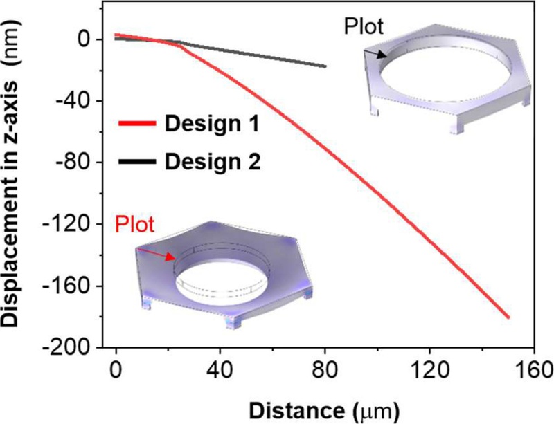
Quantitative comparison of deformation under an applied force for the two designs shown in Fig. 3. The line plots show the deformation profiles measured along the indicated lines in the corresponding design images.
Based on these experimental and numerical results, Design 2 was selected as the optimized device geometry for high-aspect-ratio nanowire patterning. This controlled mechanical effect on the motion of liquid-air interfaces is critical for converting the through-hole geometry into continuous polymeric nanowire patterns with high aspect ratios.
3.3 Fabrication of polymeric nanowire patterns
Using the optimized device, we demonstrated the formation of polymeric nanowires from a suspension of 500 nm-diameter polystyrene particles. The particle suspension was diluted to 1/15 of the original concentration, and 0.05% Pluronic F-127 surfactant was used to improve particle dispersion and suppress uncontrolled aggregation during evaporation. Moreover, the surfactant allows foam generation and retards the rupture of the nanoscale thin film. After patterning, top-view microscopy showed that the polymeric particles were assembled into regular line patterns following the periodic geometry of the through-hole device (Fig. 5(a)). The magnified microscopy image further revealed that the line patterns were formed around the supporting posts and connected neighboring through-hole units (Fig. 5(b)). These results confirm that the optimized foam-based nanopatterning device can guide polymeric particles into narrow and continuous pathways rather than leaving randomly distributed residues on the substrate.
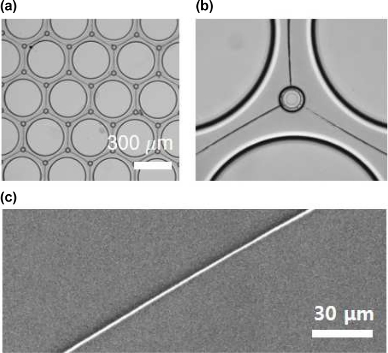
Images showing the alignment of 500 nm-diameter particles. (a) Top-view microscopy image of the resulting pattern. (b) Magnified microscopy image of the nanowire patterns formed around a post. (c) SEM image confirming single-particle-wide nanowire formation, resulting in nanowire patterns with a width of 500 nm and a length of approximately 300 µm.
SEM imaging provided direct evidence of nanoscale line formation. As shown in Fig. 5(c), the resulting pattern consisted of a single-particle-wide arrangement of 500 nm-diameter particles. The line was continuous over a long distance, with a width of approximately 500 nm and a length of approximately 300 µm. This corresponds to an aspect ratio of approximately 600, demonstrating the capability of the foam-based nanopatterning process to generate long, narrow, and well-aligned polymeric nanowires. Importantly, the width of the nanowire was defined by the particle diameter rather than by the microscale dimensions of the through-hole device, highlighting the ability of evaporation-guided assembly to bridge microscale template structures and nanoscale pattern formation.
Finally, we explored reactive ion etching as a post-patterning strategy to further increase the aspect ratio of the polymeric nanowire patterns. The schematic in Fig. 6(a) illustrates that plasma etching can reduce the lateral dimension of the preformed polymer pattern while preserving its overall line-shaped geometry. Time-dependent microscopy images after 20, 40, and 60 min of etching show a gradual reduction in the apparent width of the polymeric line patterns (Fig. 6(b)). Quantitative analysis confirmed that the nanowire width decreased monotonically with increasing etching time (Fig. 6(c)). Although prolonged etching can cause delamination or increased non-uniformity in the polymeric structures, these results suggest that the nanowire width can be further tuned by post-processing after foam-based nanopatterning. For practical manufacturing of nanowires, further optimization of parameters such as plasma power and gas type should be considered in future studies.
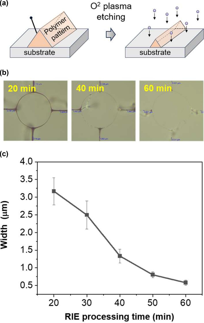
Potential strategy for further increasing the aspect ratio of polymeric nanowire patterns formed by foam-based nanopatterning. (a) Schematic illustration showing RIE to make the resulting patterns smaller. (b) Top-view microscopy of the pattern after RIE with varied processing times (c) Quantitative analysis of nanowire width as a function of RIE processing time.
The resulting polymeric nanowire patterns can provide practical structural advantages for sensor-related applications because their long, narrow, and continuous geometry offers large interfacial contact areas and one-dimensional pathways for electrical, optical, chemical, or biological interactions. For example, such dimensionally tunable polymeric nanowires could be used as functional or template structures for constructing nanofluidic channels for biosensing applications, flexible sensor interfaces for wearable devices, and photonic sensors based on perovskite or structural-color materials.
4. CONCLUSIONS
In conclusion, the proposed foam-based nanopatterning method successfully produced long, narrow, and well-aligned polymeric nanowire patterns through evaporation-guided assembly within a flexible through-hole film. The optimized device geometry provided stable meniscus confinement by suppressing excessive template deformation, which was essential for continuous line formation. As a representative demonstration, 500 nm-diameter polystyrene particles were assembled into single-particle-wide nanowires with an aspect ratio of approximately 600. The additional width reduction by reactive ion etching further indicates that the pattern dimensions can be tuned after assembly. These findings demonstrate that controlled capillary confinement in a deformable template can serve as an effective route for fabricating high-aspect-ratio polymeric nanowire structures.
Acknowledgments
This work was supported by the National Research Foundation of Korea (NRF) grant funded by the Korea government (MSIT) (No. RS-2020-NR049568 and No. RS-2025-00520477).
REFERENCES
-
Y. Cui, Q. Wei, H. Park, C.M. Lieber, Nanowire nanosensors for highly sensitive and selective detection of biological and chemical species, Science 293 (2001) 1289–1292.
[https://doi.org/10.1126/science.1062711]

-
F. Patolsky, G. Zheng, C.M. Lieber, Nanowire sensors for medicine and the life sciences, Nanomedicine 1 (2006) 51–65.
[https://doi.org/10.2217/17435889.1.1.51]
-
B. He, T.J. Morrow, C.D. Keating, Nanowire sensors for multiplexed detection of biomolecules, Curr. Opin. Chem. Biol. 12 (2008) 522–528.
[https://doi.org/10.1016/j.cbpa.2008.08.027]
-
N.S. Ramgir, Y. Yang, M. Zacharias, Nanowire-based sensors, Small 6 (2010) 1705–1722.
[https://doi.org/10.1002/smll.201000972]
-
X. Liu, Y.-Z. Long, L. Liao, X. Duan, Z. Fan, Large-scale integration of semiconductor nanowires for high-performance flexible electronics, ACS Nano 6 (2012) 1888–1900.
[https://doi.org/10.1021/nn204848r]
-
L.N. Quan, J. Kang, C.-Z. Ning, P. Yang, Nanowires for photonics, Chem. Rev. 119 (2019) 9153–9169.
[https://doi.org/10.1021/acs.chemrev.9b00240]
-
H. Zhao, R. Su, L. Teng, Q. Tian, F. Han, H. Li, et al., Recent advances in flexible and wearable sensors for monitoring chemical molecules, Nanoscale 14 (2022) 1653–1669.
[https://doi.org/10.1039/D1NR06244A]
-
M.C. McAlpine, H. Ahmad, D. Wang, J.R. Heath, Highly ordered nanowire arrays on plastic substrates for ultrasensitive flexible chemical sensors, Nat. Mater. 6 (2007) 379–384.
[https://doi.org/10.1038/nmat1891]
-
M.-Y. Shen, B.-R. Li, Y.-K. Li, Silicon nanowire field-effect-transistor based biosensors: from sensitive to ultra-sensitive, Biosens. Bioelectron. 60 (2014) 101–111.
[https://doi.org/10.1016/j.bios.2014.03.057]
-
J.T. Kim, S.K. Seol, J. Pyo, J.S. Lee, J.H. Je, G. Margaritondo, Three-dimensional writing of conducting polymer nanowire arrays by meniscus-guided polymerization, Adv. Mater. 23 (2011) 1968–1970.
[https://doi.org/10.1002/adma.201004528]
-
K.S. Beckwith, S.P. Cooil, J.W. Wells, P. Sikorski, Tunable high aspect ratio polymer nanostructures for cell interfaces, Nanoscale 7 (2015) 8438–8450.
[https://doi.org/10.1039/C5NR00674K]
-
L. Brock, J. Sheng, Robust fabrication of polymeric nanowire with anodic aluminum oxide templates, Micromachines 11 (2020) 46.
[https://doi.org/10.3390/mi11010046]
-
F. Xu, Y. Zhu, Highly conductive and stretchable silver nanowire conductors, Adv. Mater. 24 (2012) 5117–5122.
[https://doi.org/10.1002/adma.201201886]
-
S.F. Abd Rahman, N.A. Yusof, M.K. Md Arshad, U. Hashim, M.N. Md Nor, M.N. Hamidon, Fabrication of silicon nanowire sensors for highly sensitive pH and DNA hybridization detection, Nanomaterials 12 (2022) 2652.
[https://doi.org/10.3390/nano12152652]
-
Y. Yang, S. Duan, H. Zhao, Advances in constructing silver nanowire-based conductive pathways for flexible and stretchable electronics, Nanoscale 14 (2022) 11484–11511.
[https://doi.org/10.1039/D2NR02475F]
-
D.J. Sirbuly, M. Law, H. Yan, P. Yang, Semiconductor nanowires for subwavelength photonics integration, J. Phys. Chem. B 109 (2005) 15190–15213.
[https://doi.org/10.1021/jp051813i]
-
D. van Dam, D.R. Abujetas, R. Paniagua-Domínguez, J.A. Sánchez-Gil, E.P.A.M. Bakkers, J.E.M. Haverkort, et al., Directional and polarized emission from nanowire arrays, Nano Lett. 15 (2015) 4557–4563.
[https://doi.org/10.1021/acs.nanolett.5b01135]
-
X.-Y. Zhu, B.-R. Wang, Y. Gu, H. Zhu, L. Chen, Q.-Q. Sun, Novel nanofluidic cells based on nanowires and nanotubes for advanced chemical and bio-sensing applications, Nanomaterials 11 (2021) 90.
[https://doi.org/10.3390/nano11010090]
-
M. Akbari-Saatlu, M. Procek, C. Mattsson, G. Thungström, H.-E. Nilsson, W. Xiong, et al., Silicon nanowires for gas sensing: a review, Nanomaterials 10 (2020) 2215.
[https://doi.org/10.3390/nano10112215]
-
T. Arjmand, M. Legallais, T.T.T. Nguyen, P. Serre, M. Vallejo-Perez, F. Morisot, et al., Functional devices from bottom-up silicon nanowires: a review, Nanomaterials 12 (2022) 1043.
[https://doi.org/10.3390/nano12071043]
-
J. Bae, R. Wu, T. Kim, Fabricating and laminating films with through-holes and engraved/protruding structures for 3D micro/nanofluidic platforms, Small Methods 7 (2023) 2300211.
[https://doi.org/10.1002/smtd.202300211]
-
Y. Chae, J. Bae, T. Kim, Direct patterning of liquid materials on flat and curved substrates using flexible molds with through-hole and post arrays, RSC Adv. 14 (2024) 31217–31226.
[https://doi.org/10.1039/D4RA05252H]