Structural, morphological, optical, and photosensing properties of Cs2TeI6 thin film synthesized by two-step dry process
This is an Open Access article distributed under the terms of the Creative Commons Attribution Non-Commercial License(https://creativecommons.org/licenses/by-nc/3.0/) which permits unrestricted non-commercial use, distribution, and reproduction in any medium, provided the original work is properly cited.
Abstract
Recently, cesium tellurium iodine (Cs2TeI6) has emerged as an inorganic halide perovskite material with potential application in optoelectronic devices due to its high absorption coefficient, suitable bandgap and because it consists of nontoxic and earth-abundant elements. However, studies on its fabrication process as well as photoresponse characteristics are limited. In this study, a simple and effective method is introduced for the synthesis of Cs2TeI6 thin films by a two-step dry process. A Cs2TeI6-based lateral photosensor was fabricated, and its photoresponse characteristics were explored under laser illuminations of four different wavelengths in the visible range: 405, 450, 520, and 655 nm. The initial photosensing results suggest potential application and can lead to more promising studies of Cs2TeI6 film in optoelectronics.
Keywords:
Cesium tellurium iodide (Cs2TeI6), Halide perovskite, Photosensing properties, Chemical vapor deposition (CVD), Lead-free, Non-solution method1. INTRODUCTION
In the field of optoelectronics, during the past decade, metal halide perovskites have received much attention from the scientific community because their significant optical and electrical properties have shown their significant potential in practical applications. However, the most important achievements have been obtained with the use of a toxic element, Pb, which limits the commercialization of the materials [1-3]. Recently, the double halide perovskite A2BX6, with the B-site of Sn/Te replacing Pb has emerged as a promising group for Pb-free alternatives [4,5]. In particular, the stability of these materials is considerably higher when an inorganic element is presented at the A-site than when an organic compound is at the A-site. One such halide perovskite material is Cs2TeI6 compound.
According to computational research by Liu et al. [6], Cs2TeI6 exhibits a high optical absorption in the entire visible-light spectrum and an appropriate bandgap for optoelectronic applications. Moreover, it is considered to have better thermodynamic stability than its counterpart A2TeI6 or other well-known perovskites, such as MAPbI3 and FAPbI3 [6]. However, the fabrication techniques of this material are relatively limited.
In experimental studies, Guo et al. [7] and Xu et al. [8] succeeded in fabricating Cs2TeI6 film through the electrospray method. Although the studies indicated that this material has good photosensitive properties, they focused on application in X-ray detection. These Cs2TeI6 films are tens of micrometers thick, making them unsuitable for thin-film optoelectronic devices. In 2020, Isabel et al. [9] reported the fabrication of Cs2TeI6 in the form of a thin film using spin-coating of mixed CsI–TeI4 solution followed by thermal annealing. However, the morphology deteriorated when many large crystals appeared on the surface of the film. Therefore, more studies are necessary to improve not only the quality but also the understanding and application of this material.
Herein, non-solution fabrication/synthesis of Cs2TeI6 thin film on a glass substrate is reported, and its characteristic parameters in photodetection are investigated. The basic properties of the as-synthesized film were investigated via X-ray diffraction (XRD), scanning electron microscopy (SEM), and ultraviolet–visible (UV-Vis) spectroscopy techniques. Then, the photosensing properties, such as current–voltage (I–V) curves under illumination, modulation of photocurrents, photosensitivity, responsivity, and response times were evaluated demonstrating the potential for application for photosensors.
2. EXPERIMENTAL PROCEDURE
In this study, 150 mg of CsI (99.9%) and 150 mg of TeI4 (99.9%) powders (Alfa Aesar, USA) were used as precursors to fabricate the Cs2TeI6 film.
The process of fabricating the Cs2TeI6 thin film involved two main steps: deposition of CsI thin film by CVD method and then the annealing of as-deposited CsI film in TeI4 ambient to synthesize the Cs2TeI6 thin film. The experimental setup for this process is shown in Fig. 1.

(a) Setup for the synthesis of CsI film by chemical vapor deposition and (b) annealing system for conversion of CsI to Cs2TeI6 film in TeI4 vapor.
In the first step, Pyrex glass substrate (20 × 20 mm) was washed several times sequentially with solutions of trichloroethylene, acetone, ethanol, and deionized water in an ultrasonic bath. CsI powder and substrate were put into a quartz tube of the CVD system at fixed positions. Inside the tube, the working pressure was maintained at approximately 3 × 10⁻² Torr; the temperatures of the CsI powder and substrate were maintained at 350 °C and 160 °C, respectively. The system was heated at a rate of 8 °C/min, and the deposition time was 10 min. It was then naturally cooled to room temperature. In the second step, CsI film was taken together with TeI4 powder in an alumina chamber and put into an insulation system. A hot plate was used to raise the temperature to 210 °C, and it was maintained for 1 h.
The structural properties of the as-synthesized materials were investigated using XRD equipment (Panalytical X’pert Pro; Cu-Ka radiation, l = 1.54178 Å) from 10° to 50° with an interval of 0.03°. The morphological properties were examined by SEM using JEOL KSM-6701F equipment with an acceleration voltage of 10 kV. The optical properties were studied in an absorption spectrum from 300 to 900 nm with an interval of 1 nm using a Cary 5000 UV-Vis-near-infrared spectrophotometer.
To investigate the photosensing properties, indium-doped tin oxide (ITO) interdigitated electrodes were fabricated on the glass surface by a photolithography method with a 5 mm gap between the electrodes (Fig. 2a), and Cs2TeI6 film was deposited on the surface of the ITO substrate. Photographs of the ITO electrodes taken by the microscope before and after the deposition of the Cs2TeI6 film are shown in Figs. 2b and 2c, respectively. A simple schematic setup for measuring the photosensing property of the Cs2TeI6-based photosensor is illustrated in Fig. 2d.
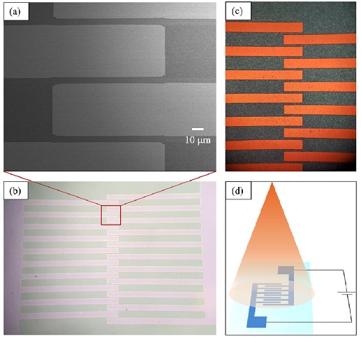
(a) SEM image of ITO electrodes showing a gap of 5 mm, (b), (c) photographs of interdigitated ITO electrodes before and after the deposition of Cs2TeI6 film, respectively, and (d) simple schematic setup for measuring photoresponse properties of Cs2TeI6-based device.
The photosensing properties were investigated in the dark as well as with the illumination from lasers with different wavelengths in visible range of 405 nm (purple), 450 nm (blue), 520 nm (green), and 655 nm (red) with adjustable output power. The measurements were performed using a probe station combined with a Keithley 4200-SCS system at room temperature.
3. RESULTS AND DISCUSSION
The crystallization of the film after the first step is shown in Fig. 3a. The cubic CsI (Pm-3m) is identified by its XRD pattern (JCPDS 01-077-2185), and there are no secondary phases in the film. The inset of Fig. 3b is a photograph of CsI that is white on a glass substrate. In the SEM images (Figs. 3b and 3c), the CsI film consists of various separated particles with a size of hundreds of nanometers, and the film has a thickness of 0.18 mm.
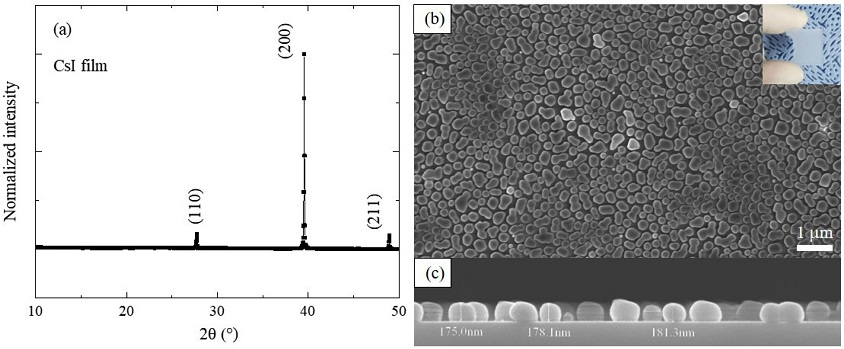
(a) XRD pattern and (b), (c) top-view and cross-sectional SEM images of CsI film deposited by chemical vapor deposition (inset is a photograph of CsI on glass substrate).
In the photograph of the Cs2TeI6 film (inset of Fig. 4b), the entire film is black after the second step. In the XRD pattern (Fig. 4a), all the peaks belong to the Cs2TeI6 phase, and characteristic peaks associated with CsI, TeI4, or other impurities are absent from the pattern. The Cs2TeI6 film has a cubic structure (Fm-3m) (JCPDS 01-073-0330). All the major peaks are also marked with the corresponding diffraction planes shown in Fig. 4a. In the top-view SEM image (Fig. 4b), the Cs2TeI6 film is continuous, uniform, and tightly packed, whereas the cross-sectional image (Fig. 4c) shows a dense and pinhole-free film with good adhesion to the substrate and a thickness of 0.35 mm.
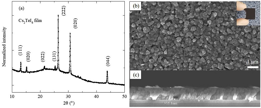
(a) XRD pattern and (b), (c) top-view and cross-sectional SEM images of Cs2TeI6 film converted from CsI film by annealing in TeI4 vapor (inset is a photograph of Cs2TeI6 on glass substrate).
The absorption coefficient of Cs2TeI6 film in the wavelength range of 300–900 nm is shown in Fig. 5a. In this range, its values are all higher than 104 cm−1. The shorter the wavelength, the higher the absorption coefficient. For wavelengths in range of 300–550 nm, all absorption coefficients are higher than 105 cm−1, reaching a maximum value of 2.38 × 105 cm−1 at λ = 325 nm.
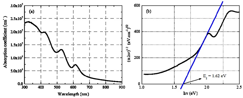
(a) Absorbance coefficient of the 0.35 mm Cs2TeI6 film and (b) Tauc plot ((abs.hn)1/2 versus hn) of absorption spectrum assuming an indirect Cs2TeI6 film bandgap.
Assuming an indirect bandgap [10-12], the Tauc method was used to determine the optical energy bandgap of the Cs2TeI6 film. The graph of the dependence of (abs.hn)0.5 on hn (Fig. 5b) shows that the bandgap of this material was 1.62 eV. This value agrees with previous experimental studies of Cs2TeI6 [8,10] that reported indirect bandgaps of 1.57 and 1.59 eV.
The absorption coefficient is of a higher order of magnitude than that of other halide perovskite films in recently published studies [13,14]. Hence, although this Cs2TeI6 material has an indirect bandgap, it has sufficiently strong optical absorption to be considered as a light-absorbing material in photoelectronic devices.
The photosensing properties of the Cs2TeI6-base photosensor were evaluated under illuminations of four different-wavelength lasers in the visible range: 405, 450, 520, and 655 nm.
First, the I–V characteristics in the dark as well as under illumination of four different-wavelength lasers at the same light intensity of 12.5 mW/cm2 for an applied voltage from −10 to +10 V were investigated and are shown in Fig. 6a. As the figure reveals, the good symmetry and linear nature of the I–V curves indicate good ohmic contact between the electrodes and Cs2TeI6 film. At the same bias voltage, it showed a significant increase in electrical current under illumination compared with under the dark condition. The logarithmic plots of all the I–V curves (inset of Fig. 6a) demonstrate more clearly the photocurrent difference at different wavelengths.

Cs2TeI6 photoresponse characterization: (a) dark and light (12.5 mW/cm2) I–V curves under different wavelength illuminations, (b) photoresponse under light pulses, and (c) photosensitivity and responsivity versus wavelength measured at 5 V bias with 12.5 mW/cm2 lasers.
To support the analysis of the photocurrent at different wavelengths further, modulation of the photocurrent was carried out with five on–off cycles of the lasers at an applied voltage of 5 V and light intensity of 12.5 mW/cm2 (Fig. 6b). The photocurrent increased to a stable value and returned to its initial value when the laser was turned off (on/off nature of photocurrent), which shows the stability as well as the repeatability characteristics of the Cs2TeI6-based device. It enables an efficient and reliable photosensor.
In the dark at a 5 V bias, the dark current had an ultralow value of approximately 1 pA, which is consistent with previous studies [7,8,10] showing that poor conductivity is an intrinsic property of Cs2TeI6 material. The photocurrent was estimated to be 1.03 × 10⁻¹⁰ A under 12.5 mW/cm2 illumination at a wavelength of 655 nm. When the wavelength decreased to 520 nm, it reached a maximum value of 9.83 × 10⁻¹⁰ A. When the wavelength continuously decreased to 450 and 405 nm, it had slightly lower values of 7.33 × 10⁻¹⁰ and 6.76 × 10⁻¹⁰ A, respectively.
The increase in photocurrent results from the creation of large numbers of charge carriers inside the film under illuminating light with energies greater than the bandgap of the Cs2TeI6 material, and the high absorption coefficient (Fig. 5a) favors this characteristic.
From the value of photocurrents, the characteristic parameters, such as photosensitivities and responsivities of a Cs2TeI6-based photosensor, can be determined. The photosensitivity (S) is defined as the change in conductivity upon illumination, as in Equation (1). The responsivity (R) is the amount of photocurrent generated per unit area per unit illumination intensity as in Equation (2). Here, P is the power density of the laser source, S is the illuminated area, and Idark, Ilight are the currents in the dark and under illumination, respectively.
| (1) |
| (2) |
In this study, these parameters were calculated from the modulation of the photocurrent in Fig. 6b and exhibited in Fig. 6c, and their change with wavelength follows the change in photocurrent with wavelength. Fig. 6c shows that the highest photosensitivity and responsivity were recorded for Cs2TeI6 film under the 520 nm laser and obtained values of 9.83 × 10⁴ % and 873 × 10−6 A/W, respectively. Moreover, the photosensitivity values at four wavelengths was sufficiently large for this Cs2TeI6-based photosensor to be applied throughout the visible-light spectrum.
The photocurrent versus time in five on/off cycles of the 520 nm laser were further measured under different intensities from 3.75 to 25 mW/cm2, as illustrated in Fig. 7a. In Fig. 7b, the dependence of the photocurrent on the light intensity follows the power law, Ip - Pq (log of Ip varies linearly to log of P), in which Ip is the non-unity exponent relation with the light intensity P. Higher photocurrents were found with the increase in the light intensity, and the value of the non-unity exponent q of 0.7 is inside the reliable range for photosensors [15,16].
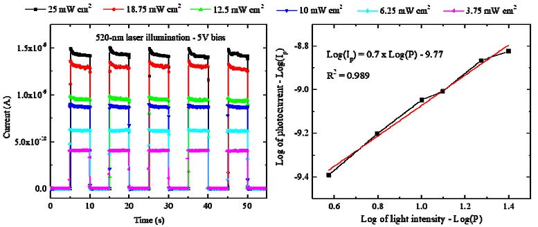
(a) Photocurrents of Cs2TeI6-based photosensor under different intensity of 520 nm laser at 5 V bias and (b) graph of log of photocurrent versus log of light intensity of the 520 nm laser.
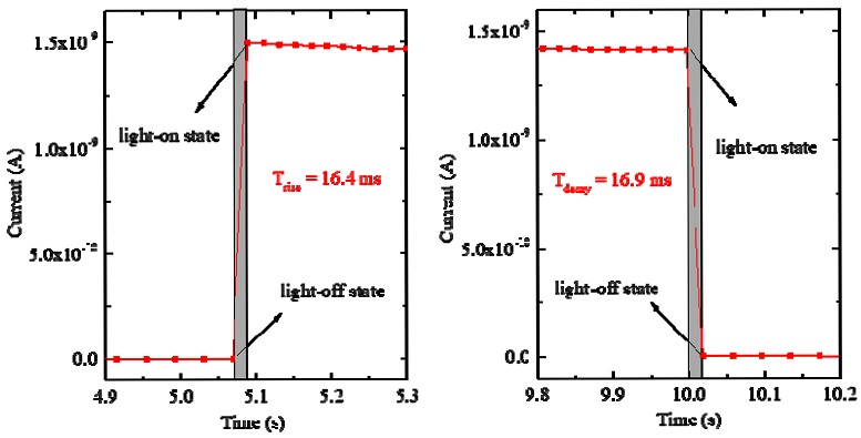
The response times, the important parameters of a photosensor, also can be determined from the modulation curve. The rise/decay times are defined as the time required to change the signal amplitude between 10% and 90% for rising/falling edges. In Fig. 8, the change in the photocurrent between on–off states of 25 mW/cm2 for a 520 nm laser at 5 V bias is shown in detail. In this figure, the values of the rise time and decay time were estimated to be approximately 16.4 and 16.9 ms, respectively. The Cs2TeI6 thin film demonstrated better response times than already reported lateral-type photosensors based on halide perovskite materials [17-22].
4. CONCLUSIONS
A Cs2TeI6 thin film was prepared, and its structure, morphology, and optical absorption were investigated to provide useful data for application to photodetection. A Cs2TeI6-based lateral photosensor on an ITO glass substrate was fabricated through a simple and effective process. Its photoresponse characteristics, such as the I–V curve, current modulation, photosensitivity, responsivity, and response times are considered very promising and warrant further studies to obtain higher values than those reported here. This study showed that the Cs2TeI6 thin film is a potential material not only for photosensors but also for other effective and environmentally friendly optoelectronic devices based on Cs2TeI6 thin films.
Acknowledgments
The work was financially supported by Kyungpook National University Development Project Research Fund, 2018.
REFERENCES
-
W. S. Yang, B. W. Park, E. H. Jung, N. J. Jeon, Y. C. Kim, D. U. Lee, S. S. Shin, J. Seo, E. K. Kim, J. H. Noh, and S. I. Seok, “Iodide management in formamidinium-lead-halide-based perovskite layers for efficient solar cells”, Science, Vol. 356, No. 6345, pp. 1376–1379, 2017.
[https://doi.org/10.1126/science.aan2301]

-
L. Zhang, L. Xu, M. Zhu, C. Li, L. Li, J. Su, and Y. Gao, “Pink all-inorganic halide perovskite nanocrystals with adjustable characteristics: Fully reversible cation exchange, improving the stability of dopant emission and light-emitting diode application”, J. Alloys Compd., Vol. 818, pp. 152913(1)-152913(11), 2020.
[https://doi.org/10.1016/j.jallcom.2019.152913]

-
Y. Wang, Y. Zhang, T. Pang, K. Sun, Z. Hu, and Y. Zhu, “Organolead halide perovskite-based metal-oxide-semiconductor structure photodetectors achieving ultrahigh detectivity”, Sol. Energy, Vol. 183, pp. 226–233, 2019.
[https://doi.org/10.1016/j.solener.2019.03.024]

-
S. Ullah, J. Wang, P. Yang, L. Liu, J. Khan, S. Yang, T. Xia, H. Guo, and Y. Chen, “Lead-free Cs2SnI6 perovskites for optoelectronic applications: Recent developements and perspectives”, Sol. RRL, Vol. 5, No. 5, pp. 2000830(1)-2000830(26), 2021.
[https://doi.org/10.1002/solr.202000830]

-
M. A. Ali, A. H. Reshak, G. Murtaza, M. A. Anazy, H. Althib, T. H. Flemban, and J. Bila, “Optoelectronic and transport properties of Rb/Cs2TeI6 defective perovskites for green energy applications”, Int. J. Energy Res., Vol. 45, No. 6, pp. 8448–8455, 2021.
[https://doi.org/10.1002/er.6378]

-
D. Liu, Q. Li, Z. Zhang, K. Wu, “Stable lead-free te-based double perovskites with tunable band gaps: A first-principles study”, New J. Chem., Vol. 43, No. 37, pp. 14892–14897, 2019.
[https://doi.org/10.1039/C9NJ03660A]

-
J. Guo, Y. Xu, W. Yang, B. Zhang, J. Dong, W. Jie, M. G. Kanatzidis, “Morphology of X-ray detector Cs2TeI6 perovskite thick films grown by electrospray method”, J. Mater. Chem. C, Vol. 7, No. 28, pp. 8712–8719, 2019.
[https://doi.org/10.1039/C9TC02022E]

-
Y. Xu, B. Jiao, T. B. Song, C. C. Stoumpos, Y. He, I. Hadar, W. Lin, W. Jie, M. G. Kanatzidis, “Zero-dimensional Cs2TeI6 perovskite: Solution-processed thick films with high X-ray sensitivity”, ACS Photonics, Vol. 6, No. 1, pp. 196–203, 2019.
[https://doi.org/10.1021/acsphotonics.8b01425]

-
I. Vázquez-Fernández, S. Mariotti, O. S. Hutter, M. Birkett, T. D. Veal, T. D. C. Hobson, L. J. Phillips, L. Danos, P. K. Nayak, H. J. Snaith, W. Xie, M. P. Sherburne, M. Asta, and K. Durose, “Vacancy-ordered double perovskite Cs2TeI6 thin films for optoelectronics”, Chem. Mater., Vol. 32, No. 15, pp. 6676–6684, 2020.
[https://doi.org/10.1021/acs.chemmater.0c02150]

-
A. E. Maughan, A. M. Ganose, M. M. Bordelon, E. M. Miller, D. O. Scanlon, J. R. Neilson, “Defect tolerance to intolerance in the Vacancy-ordered double perovskite semiconductors Cs2SnI6 and Cs2TeI6”, J. Am. Chem. Soc., Vol. 138, No. 27, pp. 8453–8464, 2016.
[https://doi.org/10.1021/jacs.6b03207]

-
Y. Cai, W. Xie, H. Ding, Y. Chen, T. Krishnamoorthy, L. H. Wong, N. Mathews, S. G. Mhaisalkar, M. Sherburne, and M. Asta, “Computational study of halide perovskite-derived A2BX6 inorganic compounds: Chemical trends in electronic structure and structural stability”, Chem. Mater., Vol. 29, No. 18, pp. 7740–7749, 2017.
[https://doi.org/10.1021/acs.chemmater.7b02013]

-
E. Y. Peresh, O. V. Zubaka, V. I. Sidei, I. E. Barchii, S. V. Kun, and A. V. Kun, “Preparation, stability regions, and properties of M2TeI6 (M = Rb, Cs, Tl) crystals”, Inorganic Materials, Vol. 38, No. 8. pp. 859–863, 2002.
[https://doi.org/10.1023/A:1019747432003]

-
H. Fujiwara, M. Kato, M. Tamakoshi, T. Miyadera, M. Chikamatsu, “Optical characteristics and operational principles of hybrid perovskite solar cells”, Phys. Status Solidi A, Vol. 215, No. 12, pp. 1–10, 2018.
[https://doi.org/10.1002/pssa.201700730]

-
P. D. Hoat, H. H. Ha, P. T. Hung, V. X. Hien, S. Lee, J. H. Lee, and Y. W. Heo, “Synthesis of Cs2SnI6 perovskite thin film by low-pressure chemical vapor deposition method”, Thin Solid Films, Vol. 732, pp. 138799(1)- 138799(8), 2021.
[https://doi.org/10.1016/j.tsf.2021.138799]

-
M. Shahid, Y. Wang, J. Yang, T. Li, Y. Xing, J. Cheng, M. Zhang, C. Wan, and W. Pan, “Indium-doped SnO2 nanobelts for high- performance transparent and flexible photosensors by a facile assembly”, Nanotechnology, Vol. 28, No. 33, pp. 335705(1)- 335705(13), 2017.
[https://doi.org/10.1088/1361-6528/aa7910]

-
W. Tian, T. Zhai, C. Zhang, S. L. Li, X. Wang, F. Liu, D. Liu, X. Cai, K. Tsukagoshi, D. Golberg, and Y. Bando, “Low-cost fully transparent ultraviolet photodetectors based on electrospun ZnO-SnO2 heterojunction nanofibers”, Adv. Mater., Vol. 25, No. 33, pp. 4625–4630, 2013.
[https://doi.org/10.1002/adma.201301828]

-
X. Han, J. Liang, J. H. Yang, K. Soni, Q. Fang, W. Wang, J. Zhang, S. Jia, A. A. Marti, Y. Zhao, and J. Lou, “Lead-free double perovskite Cs2SnX6: Facile solution synthesis and excellent stability”, Small, Vol. 15, No. 39, pp. 1–7, 2019.
[https://doi.org/10.1002/smll.201970211]

-
S. Ghosh, S. Paul, S. K. De, “Control synthesis of Air-stable morphology tunable Pb-free Cs2SnI6 perovskite nanoparticles and their photodetection properties”, Part. Part. Syst. Charact., Vol. 35, No. 9, pp. 1800199(1)-1800199(6), 2018.
[https://doi.org/10.1002/ppsc.201800199]

-
V. K. S. Hsiao, S. F. Leung, Y. C. Hsiao, P. K. Kung, Y. C. Lai, Z. H. Lin, K. N. Salama, H. N. Alshareef, Z. L. Wang, and J. H. He, “Photo-carrier extraction by triboelectricity for carrier transport layer-free photodetectors”, Nano Energy, Vol. 65, pp. 103958(1)- 103958(9), 2019.
[https://doi.org/10.1016/j.nanoen.2019.103958]

-
M. I. Saidaminov, M. A. Haque, J. Almutlaq, S. Sarmah, X. H. Miao, R. Begum, A. A. Zhumekenov, I. Dursun, N. Cho, B. Murali, O. F. Mohamed, T. Wu, and O. M. Bakr, “Inorganic lead halide perovskite single crystals: Phase-selective low-temperature growth, carrier transport properties, and self-powered photodetection”, Adv. Opt. Mater., Vol. 5, No. 2, pp. 1600704(1)-1600704(7), 2017.
[https://doi.org/10.1002/adom.201600704]

-
P. Zhu, S. Gu, X. Shen, N. Xu, Y. Tan, S. Zhuang, Y. Deng, Z. Lu, Z. Wang, and J. Zhu “Direct conversion of perovskite thin films into nanowires with kinetic control for flexible optoelectronic devices”, Nano Lett., Vol. 16, No. 2, pp. 871–876, 2016.
[https://doi.org/10.1021/acs.nanolett.5b03504]

-
X. Tang, Z. Zu, H. Shao, W. Hu, M. Zhou, M. Deng, W. Chen, Z. Zang, T. Zhu, and J. Xue, “All-inorganic perovskite CsPb(Br/I)3 nanorods for optoelectronic application”, Nanoscale, Vol. 8, No. 33, pp. 15158–15161, 2016.
[https://doi.org/10.1039/C6NR01828A]

