CMOS binary image sensor with high-sensitivity metal-oxide semiconductor field-effect transistor-type photodetector for high-speed imaging
1School of Electronic and Electrical Engineering, Kyungpook National Unversity, 80, Daehak-ro, Buk-gu, Daegu, 41566, Korea2Korea Polytechnic Robot Campus, 1, Robotcampus-ro, Yeongcheon-si, Gyeongsangbuk-do, 38839, Korea
This is an Open Access article distributed under the terms of the Creative Commons Attribution Non-Commercial License(https://creativecommons.org/licenses/by-nc/3.0/) which permits unrestricted non-commercial use, distribution, and reproduction in any medium, provided the original work is properly cited.
Abstract
In this study, we present a complementary metal-oxide-semiconductor (CMOS) binary image sensor. It can shoot an object rotating at a high-speed by using a gate/body-tied (GBT) p-channel metal-oxide-semiconductor field-effect transistor (PMOSFET)-type photodetector. The GBT PMOSFET-type photodetector amplifies the photocurrent generated by light. Therefore, it is more sensitive than a standard N+/P-substrate photodetector. A binary operation is installed in a GBT PMOSFET-type photodetector with high-sensitivity characteristics, and the high-speed operation is verified by the output image. The binary operations circuit comprise a comparator and memory of 1- bit. Thus, the binary CMOS image sensor does not require an additional analog-to-digital converter. The binary CMOS image sensor is manufactured using a standard CMOS process, and its high- speed operation is verified experimentally.
Keywords:
CMOS image sensor, Binary operation, Gate/body-tied, Photodetector, PMOSFET, High-speed operation1. INTRODUCTION
Imaging systems, such as digital still-cameras and digital video cameras that use image sensors to acquire video information effectively, are used widely. The manufacturing- process and application method can be classified largely into charge coupled device (CCD) image sensors and complementary metal-oxide-semiconductor (CMOS) image sensors. Since the latter half of the 1970s, CMOS image sensors have attracted attention owing to their capability to overcome technical issues such as noise, which are generally weak spots, and advantages such as low price, low power consumption, and superior integration. As a result, research involving modern CMOS image sensors is currently being conducted [1–3]. Sensitivity, high-speed, and dynamic range are the key study subjects for CMOS image sensors. The number of frames per second (fps) is one of the features of CMOS image sensors. An image consists of several still screens. A frame is a paused image in this context. The fps value is adjusted based on the number of frames in a second of video. The higher the fps value, the smoother the video is when it is played. A typical image has approximately 30 fps, and a very large fps value is used during high-speed shooting. The operating speed of the read-out circuit, which is composed of an amplifier and an analog-to-digital converter (ADC), is limited by the conversion speed of the ADC. Research on the development of binary image sensors is being pursued actively to overcome the drawbacks of conventional CMOS image sensors [4–8].
A CMOS binary image sensor that uses a built-in GBT PMOSFET-type photodetector with high-sensitivity characteristics operates at high speed by binarizing the output of a pixel similarly as in a read-out operation in a normal memory. It does not require an additional ADC. It consists of a high-speed logic operation-based comparator and a simple circuit using memory. Therefore, it operate with low power consumption [9]. The CMOS binary image sensor with a built-in GBT PMOSFET-type photodetector is designed herein, manufactured using the 0.35-μm standard CMOS process, and evaluated by measuring its characteristics.
2. PRINCIPLE OF OPERATION
2.1 Active pixel sensor with N+/P-substrate photodetector
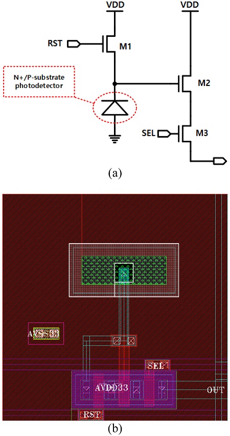
Fig. 1(a) shows the schematic of an active pixel sensor (APS) with an N+/P-substrate photodetector. The APS consists of three n-channel MOSFETs (NMOSFET) and the N+/P-substrate photodetector. As a reset transistor, the NMOSFET’s M1 transistor resets the signal voltage of the N+/P-substrate photodetector to the reference voltage. Meanwhile, the M2 transistor functions as a source follower to amplify the voltage. The M3 transistor is a select transistor that connects the output node of the APS to the voltage of the N+/P-substrate photodetector. Fig. 1(b) shows the layout of an APS with the N+/P-substrate photodetector.
2.2 APS with GBT PMOSFET-type photodetector
Fig. 2 (a) shows the schematic of an APS with a GBT PMOSFET-type photodetector. The gate node of this photodetector is designed to be physically tied with the body node. In addition, the structure of an APS using a GBT PMOSFET-type photodetector is similar to that of an APS using an N+/P-substrate photodetector. Fig. 2(b) shows a cross-section of the GBT PMOSFET-type photodetector. The area of this photodetector except the gate is shielded by a metal wire. The gate consists of polysilicon. As a result, light strikes only the gate region of the photodetector. Some photons with short wavelength (450 nm) are absorbed in the polysilicon gate, resulting in the reduction of sensitivity, while photons with long wavelength (650 nm) are mostly absorbed by the substrate. This causes the formation of electron–hole pairs in the depletion region of the P substrate. The poly silicon gate and P substrate provide an electric field that separates electron–hole pairs. The electron in a separated electron–hole pair shifts to the N well, whereas the hole shifts to the P substrate. Electrons generated by incident light accumulate in the N well. This lowers the voltage of the N well and the gate, which is physically connected to the N well. Therefore, the GBT PMOSFET-type photodetector amplifies the photocurrent generated by the incident light and displays high sensitivity [10–12]. Fig. 2(c) shows the layout of an APS with a GBT PMOSFET-type photodetector.
2.3 CMOS binary image sensor
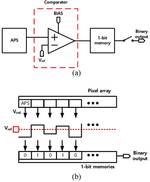
Fig. 3(a) shows a schematic of the unit column read-out circuit of the CMOS binary image sensor manufactured using the GBT PMOSFET-type photodetector. Fig. 3(b) shows the binary processing system of this binary image sensor. The CMOS binary image sensor comprises a pixel array made with a GBT PMOSFET-type photodetector, a binary comparator, and memory of 1 bit. The read-out circuit of a current CMOS image sensor comprises an amplifier and an ADC. Furthermore, the signal processing circuit is more complex than that in a CMOS binary image sensor. An analog signal is converted to a digital signal by an ADC. The conversion speed limits the operating speed. The voltage VOUT, which contains the incident light signal, reaches the input of the comparator. The voltage input of the comparator is converted to “1” if it is larger than Vref and to “0” if it is smaller. This enables high-speed operation.
3. RESULTS AND DISCUSSIONS
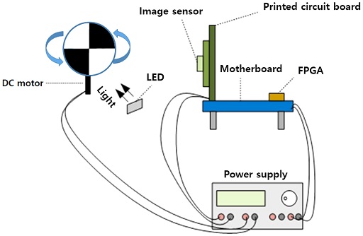
Fig. 4 shows the measurement environment for image acquisition of the CMOS binary image sensor. The power supply provides the mother board, PCB, and DC motor with their supply voltage. The image sensor is powered by the voltage and current supplied by the PCB and motherboard, and the input signal is supplied by the FPGA linked to the motherboard. We use black and white circles for the subject, and irradiate the light using LEDs. The subject rotates at high speed according to the voltage supplied to the DC motor. The output voltage of the pixel varies according to the amount of light reflected from the subject and enters the image sensor. A read-out circuit converts the pixel output voltage to a binary image.
Fig. 5(a) shows the simulation result of the photon transfer curve. Simulations were performed using Vref = 1.0 V, VBias = 1.4 V, and integration time = 500 μs. The output voltage of the APS using the GBT PMOSFET-type photodetector is saturated at a photocurrent of about 10 pA. As a result, it displays substantial sensitivity even in low light. The measurement results of the CMOS image sensor utilizing the N+/P- substrate photodetector and those of the CMOS image sensor employing the GBT PMOSFET-type photodetector are shown in Fig. 5(b) and (c), respectively. The DC motor’s voltage is supplied by the power supply, the subject’s rotation speed is 1000 rpm, and the CMOS image sensor’s frame rate is set to 100 fps to acquire the image of the subject. It is verified by measurement that the GBT PMOSFET-type photodetector has a high sensitivity.
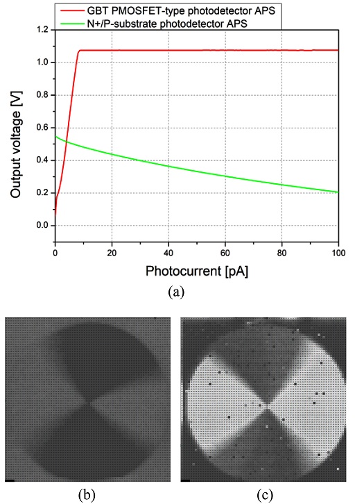
(a) Simulation results of the photon transfer curve, (b) measurement result of CMOS image sensor using N+/P-substrate photodetector for an object rotating at 1000 rpm, and (c) measurement result of CMOS image sensor using GBT PMOSFET-type photodetector for the object rotating at 1000 rpm.
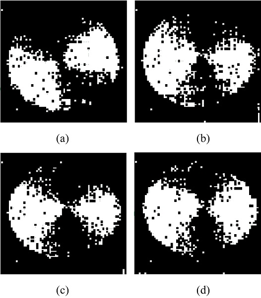
Fig. 6 is an image obtained by adjusting the fps of the image sensor using an existing CMOS image sensor for a subject rotating a high speed. The voltage of the DC motor is adjusted to rotate the subject at 8000 rpm, and images of the subject are obtained at 500, 1000, 1500, and 2000 fps to verify the high-speed operation of the CMOS image sensor. It is demonstrated qualitatively that the present CMOS image sensor’s integration time decreases, and that the read-out circuit’s conversion speed by the analog-to-digital converter cannot match.
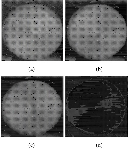
Measurement results of conventional CMOS image sensors for the object rotating at 8000 rpm, at (a) 500, (b) 1000, (c) 1500, and (d) 2000 fps.
Fig. 7 is an image obtained by adjusting the fps of the image sensor using a CMOS binary image sensor for a subject rotating at a high speed. To verify the high-speed operation of this image sensor, the voltage of the DC motor is adjusted to rotate the subject at 8000 rpm, and the subject is operated at 500, 1000, 1500, and 2000 fps to acquire its image. Because the output image is a binary image that is output by assigning “0” and “1” according to the Vref of the comparator, it is verified qualitatively by measurement that this image sensor is suitable for high-speed operation.
4. CONCLUSIONS
The simulation and measurement results verify that the CMOS binary image sensor with a built-in GBT PMOSFET-type photodetector is suitable for high-speed operation. The measurement verifies that this binary image sensor can shoot a subject rotating at a high-speed at up to 2000 fps. The binary image sensor can shoot moving objects at high-speed, and is likely to be used in various industrial fields, such as drones and unmanned surveillance cameras.
Acknowledgments
This research was supported by the Samsung Electronics Company, Basic Science Research Program through the National Research Foundation of Korea (NRF), funded by the Ministry of Education (2018R1D1A3B0704995213), and the Integrated Circuit Design Education Center (IDEC) in Korea.
REFERENCES
-
R. H. Nixon, S. E. Kemeny, B. Pain, C. O. Staller, and E. R. Fossum, “256 × 256 CMOS active pixel sensor camera-on-a-chip”, IEEE J. Solid-State Circuits, Vol. 31, No. 12, pp. 2046–2050, 1996.
[https://doi.org/10.1109/4.545830]

-
E. R. Fossum, “CMOS image sensors: electronic camera-on-a-chip”, IEEE Trans. Electron Devices, Vol. 44, No. 10, pp. 1689–1698, 1997.
[https://doi.org/10.1109/16.628824]

-
M. Bigas, E. Cabruja, J. Forest, and J. Salvi, “Review of CMOS image sensors”, Microelectronics J., Vol. 37, No. 5, pp. 433–451, 2006.
[https://doi.org/10.1016/j.mejo.2005.07.002]

-
Y. Oike, M. Ikeda, and K. Asada, “A CMOS image sensor for high-speed active range finding using column-parallel time-domain ADC and position encoder”, IEEE Trans. Electron Devices, Vol. 50, No. 1, pp. 152–158, 2003.
[https://doi.org/10.1109/TED.2002.806967]

- H. Kwen, S. H. Kim, J. Lee, P. Choi, and J. K. Shin, “Simulation of high-speed and low-power CMOS binary image sensor based on gate/body-tied PMOSFET-type photodetector using double-tail comparator,” J. Sens. Sci. Technol., Vol. 29, No. 2, pp. 82–88, 2020.
- H. Kwen, J. Jang, P. Choi, and J. K. Shin, “CMOS binary image sensor using double-tail comparator with high-speed and low-power consumption,” J. Sens. Sci. Technol., Vol. 30, No. 2, pp. 82–87, 2021.
- S. Yoshimura, T. Sugiyama, K. Yonemot, and K. Ueda, “A 48kframe/s CMOS image sensor for real-time 3-D sensing and motion detection”, Dig. Tech. Pap. - IEEE Int. Solid-State Circuits Conf., Vol. 26, No. 3, pp. 94–95, 2001.
- S. H. Kim, H. Kwen, J. Jang, Y. M. Kim, and J. K. Shin, “2500 fps high-speed binary CMOS image sensor using gate/body-tied type high-sensitivity photodetector,” J. Sens. Sci. Technol., Vol. 30, No. 1, pp. 61–65, 2021.
-
B. S. Choi, S. H. Kim, J. Lee, C. W. Oh, S. H. Seo, and J. K. Shin, “Complementary metal oxide semiconductor image sensor using gate/body-tied P-channel metal oxide semiconductor field effect transistor-type photodetector for high-speed binary operation”, Sensors Mater., Vol. 30, No. 1, pp. 129–134, 2018.
[https://doi.org/10.18494/SAM.2018.1643]

- S. H. Seo, K. D. Kim, M. W. Seo, J. S. Kong, J. K. Shin, and P. Choi, “Optical characteristics of an N-Well/gate-tied PMOSFET-type photodetector with built-in transfer gate for CMOS image sensor”, Sensors Mater., Vol. 19, No. 7, pp. 435–444, 2007.
-
W. Zhang and M. Chan, “A high gain N-Well/Gate tied PMOSFET image sensor fabricated from a standard CMOS process”, IEEE Trans. Electron Devices, Vol. 48, No. 6, pp. 1097–1102, 2001.
[https://doi.org/10.1109/16.925233]

- J. Lee, B. S. Choi, D. Seong, J. Lee, S. H. Kim, J. Lee, J. K. Shin, and P. Choi, “CMOS binary image sensor with gate/body-tied PMOSFET-type photodetector for low-power and low-noise operation,” J. Sens. Sci. Technol., Vol. 27, No. 6, pp. 362–367, 2018.
