Effects of Transfer Gate on the Photocurrent Characteristics of Gate/Body-Tied MOSFET-Type Photodetector
This is an Open Access article distributed under the terms of the Creative Commons Attribution Non-Commercial License(https://creativecommons.org/licenses/by-nc/3.0/) which permits unrestricted non-commercial use, distribution, and reproduction in any medium, provided the original work is properly cited.
Abstract
In this study, we studied the effects of transfer gate on the photocurrent characteristics of gate/body-tied (GBT) metal-oxide semiconductor field-effect transistor (MOSFET)-type photodetector. The GBT MOSFET-type photodetector has high sensitivity owing to the amplifying characteristic of the photocurrent generated by light. The transfer gate controls the flow of photocurrent by controlling the barrier to holes, thereby varying the sensitivity of the photodetector. The presented GBT MOSFET-type photodetector using a built-in transfer gate was designed and fabricated via a 0.18-μm standard complementary metal-oxide-semiconductor (CMOS) process. Using a laser diode, the photocurrent was measured according to the wavelength of the incident light by adjusting the voltage of the transfer gate. Variable sensitivity of the presented GBT MOSFET-type photodetector was experimentally confirmed by adjusting the transfer gate voltage in the range of 405 nm to 980 nm.
Keywords:
Photodetector, Gate/body-tied, Transfer gate, MOSFET, Variable sensitivity, Near-infrared region1. INTRODUCTION
The image sensor is a semiconductor sensor that obtains image information by using the photoelectric effect of light coming through an optical lens. Recently, owing to the advantages of unit pixel size, image resolution, and low power consumption, CMOS image sensors are being used in various fields, and related research is being actively conducted [1-7]. The important characteristics of the image sensor are sensitivity and dynamic range. Sensitivity is the amount of electrical signal generated by the sensor in proportion to the amount of light incident on the image sensor. The dynamic range refers to the ratio of the minimum illuminance and the ratio of the maximum illuminance at which the image sensor can express image information. Accordingly, a photodetector with high sensitivity and a wide dynamic range is being actively studied [8-11].
In this study, we have presented a GBT MOSFET-type photodetector using a built-in transfer gate having a small pixel area and high sensitivity. The GBT MOSFET-type photodetector exhibits high sensitivity, due to its inherent amplifying characteristics [12-15]. Transfer gate could be used to control the flow of photocurrent in the GBT MOSFET-type photodetector according to a voltage applied to the transfer gate, thereby varying the sensitivity of the photodetector.
In this study, we also studied the effects of the transfer gate on the photocurrent characteristics of the GBT MOSFET-type photodetector. The transfer gate controls the flow of photocurrent by controlling the barrier to holes [16]. A GBT MOSFET-type photodetector using a built-in transfer gate was designed and fabricated via a 0.18-μm standard CMOS process. In the presented GBT MOSFET-type photodetector, we measured the photocurrent according to the wavelength of the incident light by controlling the transfer gate voltage in the range of 405 nm - 980 nm.
2. PRINCIPLE OF OPERATION
Fig. 1 (a) depicts a cross-section of the GBT MOSFET-type photodetector using a built-in transfer gate. Although the structure is similar to that of the conventional GBT MOSFET-type photodetector, the presented photodetector has another transfer gate that can control the generated photocurrent. In the presented GBT MOSFET-type photodetector using a built-in transfer gate, the area except the gate of the conventional GBT MOSFET-type photodetector is shielded using a metal wire. The gate consists of a polysilicon. As a result, light strikes only the gate region of the conventional GBT MOSFET-type photodetector. Some photons with short wavelengths are absorbed in the polysilicon gate, further reducing the sensitivity, whereas photons with long wavelengths are mostly absorbed by the substrate. The incident light forms electron-hole pairs in the depletion region between the N-well and the P substrate and in the depletion region between the drain and source regions of a conventional GBT MOSFET-type photodetector. Electron-hole pairs are formed in the depletion region between the N-well and P substrate, electrons migrate to the N-well and holes migrate to the P substrate. The electrons generated by the incident light are accumulated in the N-well, the voltage of the N-well is lowered by the accumulated electrons, and the voltage of the gate physically tied to the N-well is also reduced. In addition, the electrons among the electron-hole pairs generated in the depletion region between the P+ region and the N-well of the conventional GBT MOSFET-type photodetector move to the N-well and accumulate. Holes drift toward the channel of a conventional GBT MOSFET-type photodetector with a low potential barrier to holes. The transfer gate controls the flow of photocurrent by controlling the barrier to holes. By adjusting the voltage of this transfer gate, the sensitivity of the GBT MOSFET-type photodetector can be controlled. Fig. 1 (b) depicts the symbol of the GBT MOSFET-type photodetector using a built-in transfer gate. The drain of the conventional GBT MOSFET-type photodetector and the source of the transfer gate are connected, and the body is also tied together.
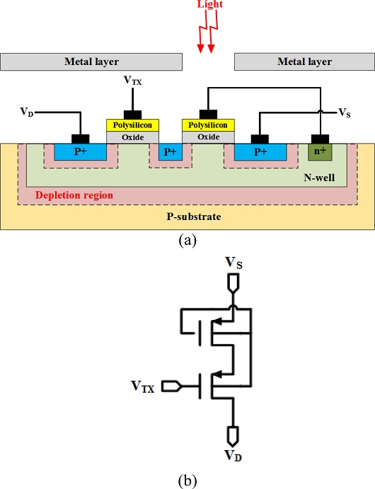
(a) Cross-section of the GBT MOSFET-type photodetector using a built-in transfer gate, (b) symbol of the GBT MOSFET-type photodetector using a built-in transfer gate.
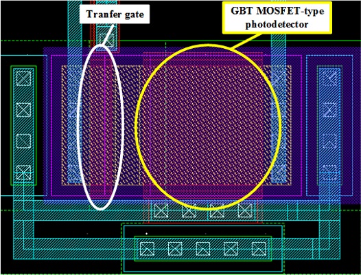
Fig. 2 depicts the layout of the GBT MOSFET-type photodetector using a built-in transfer gate. Aspect ratio of the GBT MOSFET-type photodetector is 2 μm/2 μm, whereas that of the transfer gate is 2 μm/0.35 μm.
3. EXPERIMENTAL RESULTS AND DISCUSSIONS
Fig. 3 (a) depicts the fabricated chip and Fig 3 (b) depicts the experimental environment using probe station for photocurrent measurement of the photodetector. Seven laser diodes with wavelengths of 405 nm, 520 nm, 650 nm, 780 nm, 850 nm, 940 nm, and 980 nm were used as incident light source. A collimator was used to focus the light emitted from the laser diode on the chip. The chip was fabricated via a 0.18-μm standard CMOS process.
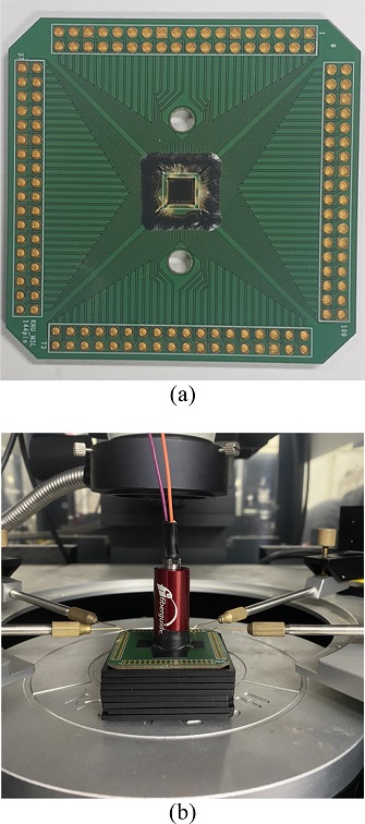
(a) The fabricated chip and (b) the experimental environment using probe station for photocurrent measurement of the photodetector.
Fig. 4 depicts the variation of the photocurrent with the source voltage as a function of the transfer gate voltage (VTX) to optimize the operating voltage of the transfer gate in the presented GBT MOSFET-type photodetector. At 780 nm wavelength, the optical power was 10 μW, and the voltage of the transfer gate was increased from 0 – 1 V. It was confirmed through measurement that the saturated source voltage of the photocurrent flowing through the GBT MOSFET-type photodetector using a built-in transfer gate increases as the voltage of VTX increases.
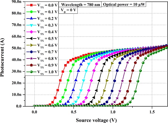
Variation of the photocurrent with the source voltage as a function of the transfer gate voltage (VTX) .
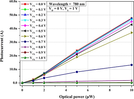
Fig. 5 depicts the variation of photocurrent with optical power as a function of transfer gate voltage. VTX was measured from 0 – 1 V, and the source voltage of the presented GBT MOSFET-type photodetector was set at 1 V to measure the photocurrent. At a wavelength of 780 nm, the light was emitted with five optical powers: 0 μW, 1 μW, 2 μW, 5 μW, and 10 μW. It was confirmed through measurements that the photocurrent of the presented GBT MOSFET-type photodetector decreased as VTX increased. Therefore, we can see that the slope of the curve, which is proportional to the sensitivity of the photodetector, decreases as VTX increases.
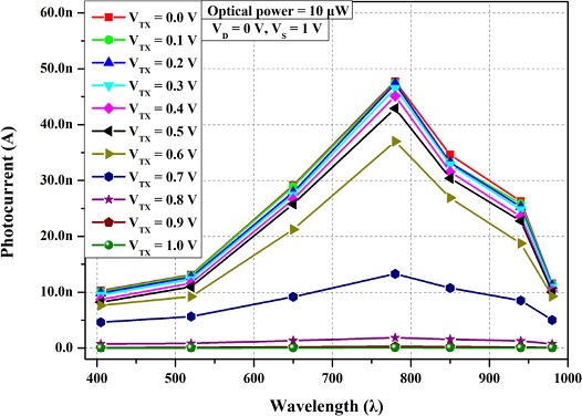
Fig. 6 depicts the variation of photocurrent with wavelength as a function of transfer gate voltage. VTX was varied from 0 – 1 V, and the source voltage of the presented GBT MOSFET-type photodetector was set at 1 V to measure the photocurrent. In addition, the optical power was set at 10 μW. As VTX decreases, the photocurrent of the presented GBT MOSFET-type photodetector varied at a wavelength of 405 – 980 nm, and we can see that the photocurrent is the largest at a wavelength of 780 nm. Below 780 nm, as the wavelength decreases, more photons are absorbed near the surface, resulting in the decrease of photocurrent. Above 780 nm, as the wavelength increases, absorption coefficient decreases, resulting in the decrease of photocurrent.
4. CONCLUSIONS
In this study, the effects of transfer gate on the photocurrent characteristics of the GBT MOSFET-type photodetector were studied. The transfer gate controls the flow of photocurrent by controlling the barrier to holes, thereby varying the sensitivity of the photodetector. A GBT MOSFET-type photodetector using a built-in transfer gate was designed and fabricated using a 0.18-μm standard CMOS process. Photocurrent characteristics according to the source voltage of the presented GBT MOSFET-type photodetector, optical power, and wavelength, were evaluated as a function of VTX through measurements. As a result, it was confirmed that the sensitivity decreases as the transfer gate voltage increases. In addition, it was confirmed that the photocurrent is largest at a wavelength of 780 nm.
Acknowledgments
This research was supported by the Samsung Electronics Company, Basic Science Research Program through the National Research Foundation of Korea (NRF) funded by the Ministry of Education (2018R1D1A3B0704995213), and the Integrated Circuit Design Education Center (IDEC) in Korea, and we are grateful for these supports.
REFERENCES
-
E. R. Fossum and S. Member, “CMOS Image Sensors : Electronic Camera-On-A-Chip”, IEEE Trans. Electron. Devices, Vol. 44, No. 10, pp. 1689-1698, 1997.
[https://doi.org/10.1109/16.628824]

-
S. Mehta, A. Patel, and J. Mehta, “CCD or CMOS Image sensor for photography”, 2015 Int. Conf. Commun. Signal Process. ICCSP 2015, pp. 291-294, Melmaruvathur, India, 2015.
[https://doi.org/10.1109/ICCSP.2015.7322890]

- B. S. Carlson, “Comparison of Modern CCD and CMOS Image Sensor Technologies and Systems for Low Resolution Imaging”, Proc. IEEE Sens., Vol. 1, No. 1, pp. 171-176, 2002.
-
M. Bigas, E. Cabruja, J. Forest, and J. Salvi, “Review of CMOS image sensors”, Microelectron. J., Vol. 37, No. 5, pp. 433-451, 2006.
[https://doi.org/10.1016/j.mejo.2005.07.002]

-
B. Luo, L. Yan, and F. Yang, “Research of noise suppression for CMOS image sensor”, 2010 Int. Conf. Meas. Technol. Mechatron. Autom. ICMTMA 2010, Vol. 2, pp. 1100-1103, Changsha City, China, 2010.
[https://doi.org/10.1109/ICMTMA.2010.261]

- J. Lee, B. S. Choi, D. Seong, J. Lee, S. H. Kim, J. Lee, J.-K. Shin, and P. Choi “CMOS Binary Image Sensor with Gate/Body-Tied PMOSFET-Type Photodetector for Low-Power and Low-Noise Operation,” J. Sens. Sci. Technol., Vol. 27, No. 6, pp. 362-367, 2018.
-
H. Kwen, S. H. Kim, J. Lee, P. Choi, and J.-K. Shin, “Simulation of High-Speed and Low-Power CMOS Binary Image Sensor Based on Gate/Body-Tied PMOSFET-Type Photodetector Using Double-Tail Comparator,” J. Sens. Sci. Technol., Vol. 29, No. 2, pp. 82-88, 2020.
[https://doi.org/10.5369/JSST.2020.29.2.82]

-
H. Alaibakhsh and M. A. Karami, “Analytical Modeling of Pinning Process in Pinned Photodiodes”, IEEE Trans. Electron. Devices, Vol. 65, No. 10, pp. 4262-4368, 2018.
[https://doi.org/10.1109/TED.2018.2862251]

- J. H. Park, H. Kim, I. S. Wang, and J. K. Shin, “Quantumwired MOSFET photodetector fabricated by conventional photolithography on SOI substrate”, 2004 4th IEEE Conf. Nanotechnol., pp. 425-427, Munich, Germany, 2004.
-
E. R. Fossum and D. B. Hondongwa, “A review of the pinned photodiode for CCD and CMOS image sensors”, IEEE J. Electron. Devices Soc., Vol. 2, No. 3, pp. 33-43, 2014.
[https://doi.org/10.1109/JEDS.2014.2306412]

-
L. A. P. Santos, G. G. Araujo, F. L. Oliveira, E. F. Silva, and M. A. P. Santos, “An alternative method for using bipolar junction transistors as a radiation dosimetry detector in breast cancer treatment”, Radiat. Meas., Vol. 71, pp. 407-411, 2014.
[https://doi.org/10.1016/j.radmeas.2014.08.003]

-
W. Zhang and M. Chan, “A high gain N-Well/Gate tied PMOSFET image sensor fabricated from a standard CMOS process”, IEEE Trans. Electron Devices, Vol. 48, No. 6, pp. 1097-1102, 2001.
[https://doi.org/10.1109/16.925233]

-
S. H. Kim, H. Kwen, J. Jang, Y. M. Kim, and J. K. Shin, “2500 fps High-Speed Binary CMOS Image Sensor Using Gate/Body-Tied Type High-Sensitivity Photodetector,” J. Sens. Sci. Technol., Vol. 30, No. 1, pp. 61-65, 2021.
[https://doi.org/10.46670/JSST.2021.30.1.61]

-
J. Jang, W. Heo, J. Kong, Y. M. Kim, and J. K. Shin, “CMOS binary image sensor with high-sensitivity metal-oxide semiconductor field-effect transistor-type photodetector for high-speed imaging,” J. Sens. Sci. Technol., Vol. 30, No. 5, pp. 295-299, 2021.
[https://doi.org/10.46670/JSST.2021.30.5.295]

-
J. Jang, J. Lee, H. Kwen, S. H. Seo, P. Choi, and J. K. Shin, “Adjusting the Sensitivity of an Active Pixel Sensor Using a Gate/Body-Tied P-Channel Metal-Oxide Semiconductor Field-Effect Transistor-Type Photodetector With a Transfer Gate,” J. Sens. Sci. Technol., Vol. 30, No. 2, pp. 114-118, 2021.
[https://doi.org/10.46670/JSST.2021.30.2.114]

- S. H. Seo, K. D. Kim, M. W. Seo, J. S. Kong, J. K. Shin, and P. Choi, “Optical characteristics of an N-Well/gate-tied PMOSFET-type photodetector with built-in transfer gate for CMOS image sensor”, Sens. Mater., Vol. 19, No. 7, pp. 435-444, 2007.
