Ionic Passivation and Oxidation Dynamics for Enhanced Viability of Copper-Based On-Skin Bioelectrodes in Biological Environments
This is an Open Access article distributed under the terms of the Creative Commons Attribution Non-Commercial License(https://creativecommons.org/licenses/by-nc/3.0/) which permits unrestricted non-commercial use, distribution, and reproduction in any medium, provided the original work is properly cited.
Abstract
The integration of bioelectronic devices with the skin is a promising strategy for personalized healthcare monitoring and diagnostics. On-skin bioelectrodes hold great potential for the real-time tracking of physiological parameters. However, persistent challenges of stability and reliability have instigated exploration beyond conventional noble metals. This study focuses on the ionic passivation and oxidation dynamics of copper-based on-skin thin-film bioelectrodes. Through parylene chemical vapor deposition, we harness a controlled thin film of parylene insulation to counter the intrinsic susceptibility of copper to oxidation in the ionic environment. The results represent the relationship among the parylene insulation thickness, copper oxidation, and electrode impedance over temporal intervals. Comparative analyses indicate that the short-term stability of the copper electrode is comparable to that of the gold electrode. Therefore, we propose a cost-effective strategy for fabricating copper-based on-skin bioelectrodes by introducing enhanced ionic stability within a discernible operational timeframe. This study enriches our understanding of on-skin bioelectronics and affordable material choices for practical use in wearable healthcare devices.
Keywords:
Bioelectrodes, Ionic passivation, Copper-based, On-skin wearables1. INTRODUCTION
Significant progress in wearable bioelectronics has enabled researchers to prioritize the development of more reliable designs for practical applications in medical diagnostics and human-machine interfaces. A crucial aspect of this progress is the development of user-friendly wearable bioelectrodes, particularly on-skin bioelectrodes, which serve as vital links between research-grade wearable devices and biological tissues [1]. The seamless integration of electronic components with skin tissue has the potential to revolutionize personalized healthcare by facilitating the continuous and real-time monitoring of physiological parameters. Nevertheless, challenges persist in ensuring the thermal and/or chemical stability and reliability of on-skin bioelectrodes, posing limitations on the choice of conductive materials for chemically stable but expensive noble metals [2].
Owing to its enhanced chemical stability, which is attributed to insulating materials, copper has been applied in wearable electronics. Unlike noble metals that are inherently stable in ionic environments [3], copper relies on insulators to prevent ionic oxidation. Common insulating materials, such as Polydimethylsiloxane and Polyurethane, have been adopted for bioelectrode passivation. However, their amorphous structure necessitates a relatively thick coating (>10 μm) to block ion infiltration because the internal random structure inevitably contains pores that serve as conduits for ion penetration.
Recognizing the significance of a thin (<10 μm) bioelectrode structure as a conformal device, the demand for stability persists in copper-based on-skin electronics, even when utilizing a thin protective layer. Thin protective layers are economically advantageous alternatives to noble metals.
Our study diverges from controlled insulation approaches by embracing a crystalline insulator known for its superior ion rejection compared with nanoporous amorphous insulators. A parylene coating, which is a semi-crystalline conformal coating, was employed to create a thin-film device. The thin-film electrode structure, composed of a parylene-copper-parylene assembly, exhibits outstanding ionic insulation properties, attributed to the distinct semi-crystalline structure formed during the chemical vapor deposition process. In addition to emphasizing the electrical insulation properties of parylene, this study also investigates its potential to mitigate copper oxidation in ionic biological applications.
A comparative analysis was conducted on thin-film copper electronics with controlled thicknesses of parylene-insulating layers to investigate the effectiveness of parylene-based passivation in an ionic environment. The kinetics of copper oxidation are driven by the interaction between the ions and copper metal. Through the systematic modulation of the parylene insulation thickness, we explore the dynamics of ionic infiltration and copper oxidation across different time intervals. This study highlights the potential utility of copper-based thin-film bioelectrodes within a defined operational window.
Moreover, we provide a detailed fabrication procedure, including the step-by-step deposition of the parylene and copper layers. The ionic oxidation profile was investigated in both deionized water and phosphate-buffered saline environments by modulating the thickness of the parylene passivation layer (Fig. 1). The relationship between the insulation thickness, copper oxidation, and its effect on the electrical properties are quantitatively studied in vitro. The results show limited but significantly improved ion rejection by parylene-based passivation.
Ultimately, this research contributes to the understanding of on-skin bioelectrode behavior under ionic conditions and presents a practical and economically viable avenue for their development. We aim to suggest the potential use of copper-based on-skin bioelectrodes by achieving both a thin structure and high ion-rejection properties, which are attributed to the semi-crystalline conformal coating of parylene. Our experimental investigation on the relationship between ionic passivation and oxidation dynamics reveal the enhancement of the on-skin bioelectrode stability and its implications for the future of wearable healthcare technology.
2. EXPERIMENTAL
2.1 Preparation and characterization of the stretchable Parylene thin-film electrode
Parylene-C was purchased from Specialty Coating Systems (Singapore). Ethanol was purchased from Sigma-Aldrich. All water used was obtained from Millipore. Parylene-C was evaporated using a PDS 2010 LabCoater 2 vacuum deposition system (Specialty Coating Systems, Singapore). The metal was then evaporated using a thermal metal evaporator ( The One Science, Republic of Korea).
2.1.1 Fabrication of stretchable Parylene thin-film electrode
The glass substrates were cleaned with ethanol before use. The first layer of parylene was predeposited onto a glass substrate with a thickness of 400 nm (Fig. 2(a)). The glass substrate was laminated using a shadow mask containing micro-scale patterns (width: 5 mm) made using a paper cutter (Silhouette, Republic of Korea) (Fig. 2(b)). The copper was evaporated using a thermal metal evaporator with a thickness of 150 nm (Fig. 2(c)). The shadow mask was then carefully removed from the metal-deposited glass substrate (Fig. 2(d)). The second layer of the parylene coating was prepared with a thickness ranging from 200–800 nm (Fig. 2(e)). Finally, the thin-film parylene-metal-parylene sandwich layers were carefully peeled off the glass substrate.
2.1.2 Electrical characterization of the thin-film electrodes
An LCR meter was used to measure the impedance of the thin-film electrodes at a frequency of 1 kHz. Both ends of the serpentine-shaped micro-scale metal thin-film patterns were connected to a copper-nickel wire for ease of measurement.
2.1.3 Transfer of the parylene thin-film electrode from the sacrificial substrate to the skin tissue.
As the prepared ultra-thin electronic device is prone to deformation during the transfer procedure, the skin was pretreated with ethanol to prevent electrostatic interactions within and between the thin-film device and the skin tissue.
3. RESULTS AND DISCUSSIONS
3.1 Characterization of the copper thin film electrode
The thin-film copper electrodes were analyzed in vitro. The parylene-thickness-dependent passivation properties were also profiled. Optical and electrical experiments were performed in both non-ionic and ionic environments.
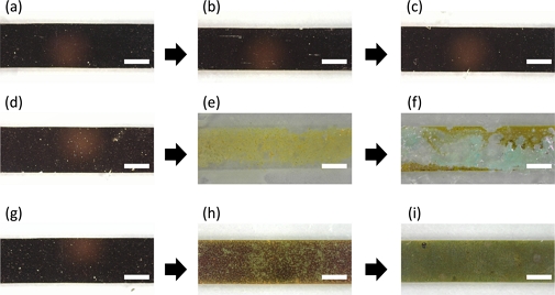
Fig. 3 shows the visual changes in the copper thin-film electrodes in three different environments: (i) a bare copper electrode in deionized water, (ii) a bare copper electrode in an ionic buffer solution, and (iii) an insulated copper electrode in an ionic buffer solution. The bare copper electrode showed no change in appearance, as no ions interacted with the copper surface (Fig. 3(a-c)). In contrast, the bare copper electrode underwent rapid oxidation in an ionic environment (ionic strength of 155 mM phosphate buffered saline). Excess amounts of the ionic buffer continuously oxidized the copper, which turned yellow and finally changed to blue when it dried. Notably, oxidation occurred on the surface of the metal; however, the copper electrode could be disconnected because of its thin structure. A clear disconnection was observed when the copper electrode was exposed to the ionic buffer for 36 h (Fig. 3(d-f)).

Oxidation dynamics and passivation effect of copper thin-film electrode exposed to the non-ionic and ionic environment for 0 hours, 12 hours, and 36 hours; (a)-(c) Bare electrode in deionized water, (d)-(f) Bare electrode in biological buffer, (g)-(i) Passivated electrode in biological buffer. (Scale bar: 2.5 mm).
As shown at the bottom of Fig. 3, the copper electrode shows a prolonged lifetime when covered by the transparent thin-film parylene, compared to the bare copper electrode. As the semi-crystal structure of the parylene layer impedes the infiltration of ions toward the surface of the copper electrode, the oxidation reaction was suppressed. Although long-term exposure to the ionic environment allowed the copper electrode to be partially oxidized even in the presence of a passivation layer, no disconnection of the electrode was observed (Fig. 3(g-i)).
Because the instability of thin-film metal electrodes originates from ionic oxidation, the impedance of the electrode showed negligible change in a non-ionic environment during the long-term (more than 2 days) investigation. The electrical investigations conform to the optical analysis, showing almost no change over time (Fig. 3(a-c)).
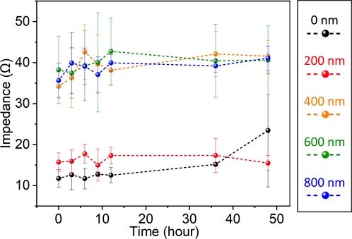
Fig. 4 shows the passivation-independent long-term stability of copper electrodes. Regardless of the thickness of the passivation layer, the variation in impedance occurred only under highly conductive levels (less than 55 Ω) in all cases. The increment in the initial impedance is caused by the infiltration of parylene vapor into the gap between the copper electrode and the bulk copper-nickel wiring. The results imply that the parylene coating with a thickness of less than 200 nm shows imperfect isolation of the electrode from the environment at 0 nm and the 200 nm-thick coating that showed a similar tendency (low impedance), unlike the samples with a coating thickness of more than 400 nm, which showed a higher impedance.
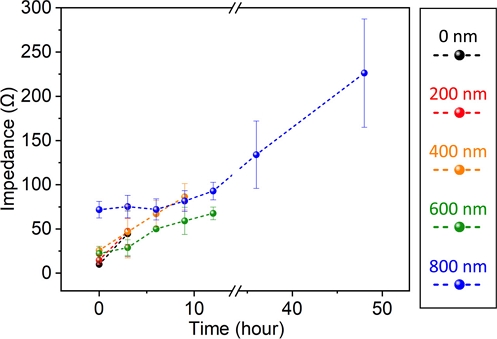
Fig. 5 shows traces of oxidation at the copper electrode. In all cases, the impedance of the bare (0–800 nm-thick coatings) increased over time. Unlike the bare electrode (0 nm-thick coatings) and 200 nm-thick coating device, which lost their electrical conductivity after 6 h of exposure to the ionic environment, the 400-, 600-, and 800 nm-thick coating devices showed prolonged lifetimes of 9 h, 12 h, and more than 48 h, respectively.

Impedance change caused by oxidation of the copper electrode with a controlled thickness of passivation layer in biological buffer.
Chemical vapor deposition of parylene-C forms an ion-blocking barrier, and the blocking rate increased as the thickness of the deposited parylene increased. The impedance change rate increased as the passivation layer thickness approached zero.
Notably, the 0 nm and 200 nm-thick coating showed almost the same stability, implying that the 200 nm-thick coating did not close the ionic pathway that allows the oxidation of copper. This result agrees with the initial impedance change observed in Fig. 4.
Even though the thickest coating (800 nm-thick) of parylene showed a relatively noticeable impedance change after sustained exposure to the ionic environment, considering real-world applications, such as a wearable device, the actual usage of the device with high conductivity can be achieved as the environment is less ionic and the frequency and duration of exposure are less.
3.2 Demonstration of the Copper thin film electrode
The potential wearable application of the device was demonstrated using a simple electronic circuit formed within a thin-film device on the human skin in vivo.
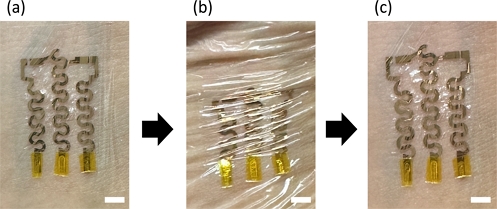
We performed an on-skin demonstration of the human skin tissue. The thin-film (less than 1 μm) copper electrode achieved conformal contact with the skin tissue (Fig. 6(a),(b)). The light and thin-film device showed almost invisible edges, so the user could barely detect the presence of the device.

Demonstration of on-skin thin-film metal electrode and its conformal contact during the deformation of the skin; (a) As-attached thin-film electrode on the human skin. (b) Deformed thin-film electrode and the skin. (c) Released thin-film electrode on the skin. (Scale bar: 5 mm).
Most importantly, the device is highly deformable owing to its low modulus. Even after extensive compression in the shear direction on the skin, the device conformed to the wrinkled structure of the skin and returned to its original shape when the skin was released from mechanical compression (Fig. 6(b),(c)).
Owing to the semi-crystalline structure of the parylene coating and its extremely thin (less than 1 μm) structure, the copper device achieved biological tissue compatibility, which is both ion tolerant and deformable.
4. CONCLUSIONS
To enhance the stability of non-noble metal-based on-skin bioelectrodes, we conducted model experiments using inexpensive copper-based thin-film electrodes and explored the relationship between the ionic passivation properties of semicrystalline parylene insulators and the ionic oxidation of copper thin-film electrodes. Chemical vapor deposition of parylene enabled the formation of a controllable thin protective barrier on the surface of the copper electrode.
Through an ultra-thin layer-by-layer vapor deposition process, we demonstrated the enhanced viability of copper-based thin-film bioelectrodes, contrary to conventional limitations arising from the susceptibility of copper to oxidation. Unlike the bare copper electrode, which lost its connection owing to ionic oxidation in an ionic buffer environment, parylene-based insulation extended the lifetime of the copper electrode. Although extremely thin (200 nm) parylene coated copper electrodes showed almost no difference in electrical stability from the bare copper electrode, a proportional enhancement in ionic passivation was observed as the thickness of parylene increased. Moreover, a relatively thick (800 nm) parylene coating showed the potential to isolate the copper electrode from the field effect of ions, as it showed almost no change in impedance for more than 6 h. Consequently, a limited yet crucial operational window was achieved by modulating the thickness of the parylene insulating layer.
Finally, we demonstrated an on-skin in vivo experiment. The thin (>1μm) copper electrode showed conformal contact to the skin tissue and mechanically compliable deformation on the wrinkled skin structure with significantly enhanced ionic stability. We believe that the simultaneous achievement of both conformal and ion-tolerant properties will help commercialize the research-level wearable device.
Acknowledgments
J. Lee conceived the idea and designed the experiments. J. Lee, G. Yun, J. Jeon, and P.T.Le. performed experiments and analyzed the data. J. Lee and G. Lim wrote the manuscript. G. Lim supervised this project. This work is financially supported by the National R&D Program through the National Research Foundation of Korea (NRF) funded by the Ministry of Science and ICT (2020M3H4A1A02084830), the NRF grant funded by the Korean government (MSIT; No. NRF-2020R1I1A3074228).
REFERENCES
-
T. Someya, Z. Bao, and G. G. Malliaras, “The rise of plastic bioelectronics”, Nature, Vol. 540, No. 7633, pp. 379-385, 2016.
[https://doi.org/10.1038/nature21004]

-
K. Liu, Y. Jiang, Z. Bao, and, X. Yan, “Skin-inspired electronics enabled by supramolecular polymeric materials”, CCS Chem., Vol. 1, No. 4, pp. 431-447, 2019.
[https://doi.org/10.31635/ccschem.019.20190048]

-
T. Someya and M. Amagai, “Toward a new generation of smart skins”, Nat. Biotechnol., Vol. 37, No. 4, pp. 382-388, 2019.
[https://doi.org/10.1038/s41587-019-0079-1]


