Asymmetric Metal–Semiconductor–Metal Al0.24Ga0.76N UV Sensors with Surface Passivation Effect Under Local Joule Heating
This is an Open Access article distributed under the terms of the Creative Commons Attribution Non-Commercial License(https://creativecommons.org/licenses/by-nc/3.0/) which permits unrestricted non-commercial use, distribution, and reproduction in any medium, provided the original work is properly cited.
Abstract
An asymmetric metal–semiconductor–metal Al0.24Ga0.76N ultraviolet (UV) sensor was fabricated, and the effects of local Joule heating were investigated. After dielectric breakdown, the current density under a reverse bias of 2.0 V was 1.1×10⁻⁹ A/cm2, significantly lower than 1.2×10⁻⁸ A/cm2 before dielectric breakdown; moreover, the Schottky behavior of the Ti/Al/Ni/Au electrode changed to ohmic behavior under forward bias. The UV-to-visible rejection ratio (UVRR) under a reverse bias of 7.0 V before dielectric breakdown was 87; however, this UVRR significantly increased to 578, in addition to providing highly reliable responsivity. Transmission electron microscopy revealed interdiffusion between adjacent layers, with nitrogen vacancies possibly formed owing to local Joule heating at the AlGaN/Ti/Al/Ni/Au interfaces. X-ray photoelectron microscopy results revealed decreases in the peak intensities of the O 1s binding energies associated with the Ga–O bond and OH-, which act as electron-trapping states on the AlGaN surface. The reduction in dark current owing to the proposed local heating method is expected to increase the sensing performance of UV optoelectronic integrated devices, such as active-pixel UV image sensors.
Keywords:
UV sensors, UV-to-visible rejection ratio, Dielectric breakdown, Joule heating1. INTRODUCTION
Nitride materials, which are direct wide-bandgap semiconductors (e.g., GaN and AlGaN), are promising candidates for applications in ultraviolet (UV) optoelectronic devices owing to their high quantum efficiency, superior solar blindness, and high radiation hardness [1-5]. Recently, sensing performances of UV optoelectronic devices have exhibited a high dark current and poor UV-to-visible rejection ratio (UVRR) and signal-to-noise ratio (SNR), attributed to their low-quality epitaxial layer and high defect density [6-8]. In addition, the considerable mismatch between the lattice constants and thermal expansion coefficients of GaN and the substrate results in a high density of threading dislocation of 108 cm−2 [9].
Various studies have been conducted to reduce the number of defects and improve the device performance by employing methods such as defect-free epitaxial growth and developing device structures exhibiting extremely low dark currents. Vertical-type UV photodetectors were fabricated on freestanding GaN substrates with low-density threading dislocations, exhibiting a high specific detectivity of more than 1012 Jones, a UVRR of 1530 at -5 V, and a high SNR of over 104 at 0 V [10]. Moreover, these UV photodetectors containing P–GaN/AlGaN/GaN heterostructures exhibited high responsivity of 2.0×10⁴ A/W and high Iph/Idark of 107 at a bias of 5.0 V [11]. Fabricated metal–insulator–semiconductor–insulator–metal UV sensors exhibited a significantly low dark current density of 5.0×10⁻⁹ A/cm2 compared to that of a metal–semiconductor–metal (MSM) UV sensor (6.2×10⁻⁷ A/cm2) [12]. Rapid thermal annealing (RTA) is recognized as a method for improving important parameters such as trap density, surface uniformity, and contact behavior that affect the device performance [13-16].
In this study, we investigated the effects of local Joule heating on the photoresponse of asymmetric MSM AlGaN UV sensors with an Al composition of 24% epitaxially grown on a sapphire substrate. The electrical and UV photoresponse characteristics were determined before and after dielectric breakdown. The cross-sections of the broken dielectric region were visualized using transmission electron microscopy (TEM) to elucidate the interdiffusion between adjacent layers. X-ray photoelectron spectroscopy (XPS) analysis was conducted to examine the chemical bonding states distributed on the AlGaN surface before and after dielectric breakdown.
2. EXPERIMENTAL
2.1 Fabrication and measurement
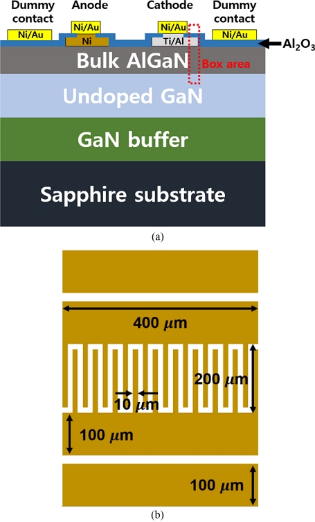
Fig. 1 shows the top and schematic cross-sectional views of the fabricated AlGaN MSM UV sensor. As shown in Fig. 1(a), the epitaxial layer was grown via metal–organic chemical vapor deposition on a (0001) sapphire substrate. The thicknesses of the undoped GaN and bulk AlGaN layer, grown using trimethylgallium, NH3, and trimethylaluminum sources, were 3.5 μm and 200 nm, respectively. For the initial cleaning, the AlGaN wafers were first rinsed with acetone and methanol for 15 and 5 min, respectively. Subsequently, the wafers were exposed to sulfuric peroxide mixture (SPM) (H2SO4:H2O2 = 3:1), standard cleaning-2 (SC2) (HCI:H2O = 1:1), and a buffered oxide etchant for 3, 3, and 1 min, respectively, to remove any contaminants. Next, photolithography was conducted using a negative photoresist (PR) to form the bottom electrode pattern. Subsequently, Ni (30 nm) and Ti/Al (30/50 nm) were deposited via electron-beam (e-beam) evaporation and lift-off. Further, a 30-nm-thick Al2O3 layer was deposited via atomic layer deposition at a processing temperature of 300 °C. A contact hole was created by dry etching using plasma. Subsequently, an ashing process was implemented to remove contaminants due to the negative PR. Then, the top electrodes and dummy pad were patterned using photolithography. Finally, Ni/Au (30/50 nm) was deposited via e-beam evaporation and lift-off.
Fig. 1(b) shows a schematic of the top view of the fabricated MSM AlGaN UV sensor. The area of this asymmetric sensor was 400×400 μm2, with a finger length of 200 μm and a finger width and space of 10 μm each. The electrical characteristics of the sensors were characterized using an Agilent HP4156C parameter analyzer, with the photoresponse characteristics recorded using a 150 W Xenon arc lamp with a monochromator (Oriel 74000) and a power meter (Newport 1930C).
2.2 Annealing method using dielectric breakdown
Fig. 2 shows a schematic three-dimensional view of the fabricated AlGaN MSM UV sensor and top-view images magnified 90× using a photomicroscope before and after dielectric breakdown. Selective annealing via the dielectric breakdown technique uses Joule heating caused by the current generated immediately after the insulator in the MSM structure breaks down locally. The current–voltage (I–V) characteristics obtained from the Ti/Al/Ni/Au ohmic metal scheme after annealing improved remarkably, demonstrating that the dielectric breakdown technique was effective for this metal scheme [17]. Therefore, the oxide (Al2O3) used for selective annealing was stacked between the Ti/Al/Ni/Au electrode and dummy pad, and a high current could flow and generate heat under a bias voltage to break down the insulating oxide film, resulting in effective annealing. Furthermore, the annealing affected the Ti/Al/Ni/Au electrode, dummy pad, and interdigitated fingers, as observed using a photomicroscope (MS TECH MST-8000C probe station).
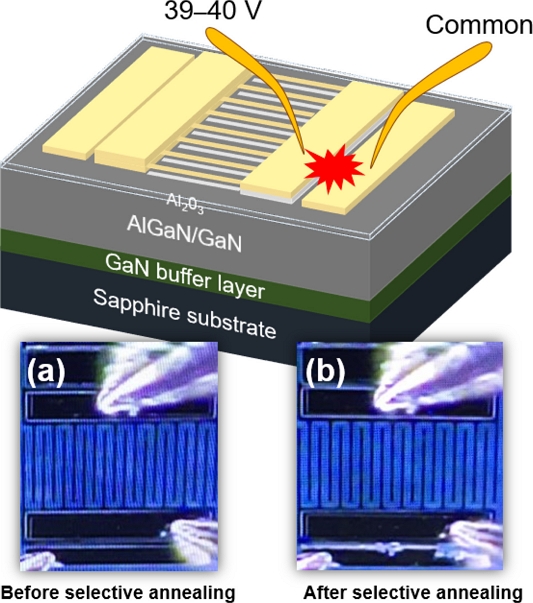
Schematic three-dimensional view of the fabricated AlGaN MSM UV sensor (top), with the image magnified 90× using a photomicroscope for investigating the surface morphological changes (a) before and (b) after dielectric breakdown.
Table 1 lists the bias conditions required for dielectric breakdown. Using a parameter analyzer, a bias voltage of 39–40 V at 0.02 V intervals was applied to the Ti/Al/Ni/Au electrode 51 times to produce a continuous annealing effect. The compliance current was set at 50 mA.
3. RESULTS AND DISCUSSIONS
3.1 Photoresponse of the MSM Al0.24Ga0.76N UV sensor
Table 2 summarizes the parameters of the photoluminescence (PL) spectra obtained from the epitaxial AlGaN wafer at room temperature before fabricating the MSM UV sensor. The full width at half maximum (FWHM) of the AlGaN wafers with Al compositions of 39, 33, and 24% were 18, 13, and 6 nm, respectively, yielding a poor-quality epitaxial layer, attributed to the large differences in physical properties, such as the lattice constant, thermal expansion coefficients, and growth temperatures, with respect to those of binary compounds such as GaN. In addition, the quality of the AlGaN layer grown on the GaN buffer is inferior to that of a single GaN layer, and the high Al content increases the lattice mismatch between AlGaN and GaN, thereby deteriorating the quality of the AlGaN epitaxial layer. In this study, an AlGaN wafer with 24% Al content was used. The bandgap (Eg) as a function of the Al composition was obtained as previously reported [18].
Fig. 3 shows the dark and UV photoresponses of the MSM-AlGaN UV sensor. Additionally, the cut-off wavelengths of Al0.25Ga0.76N and GaN are 316 and 365 nm, corresponding to Eg values of 3.92 and 3.65 eV, respectively, yielding a high concentration of electron–hole pairs (EHPs) generated under UV irradiation. Developing a highly sensitive dual-wavelength UV sensor and photodetector is possible for active-pixel UV image sensing if the dark current and UVRR can be improved. The I–V characteristics of the MSM AlGaN UV sensor were asymmetric owing to the work function difference between the Ni/Au (5.04 eV) and Ti/Al/Ni/Au (4.33 eV) electrodes.
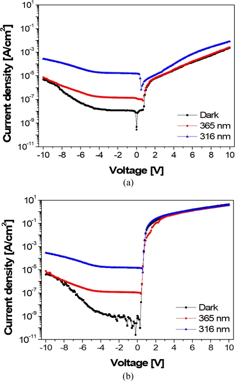
Dark and UV photo responses of the MSM AlGaN UV sensor (a) before and (b) after dielectric breakdown.
Under a forward bias of 4.0 V and dark conditions, as shown in Fig. 3(a), the current density before dielectric breakdown was 3.0×10⁻⁵ A/cm2, drastically increasing to 0.8 A/cm2 after dielectric breakdown. This result indicates that the Schottky behavior of the Ti/Al/Ni/Au electrode changed to near-ohmic behavior owing to Joule heating without RTA, attributed to the formation of N vacancies (VN) owing to the interdiffusion of elements such as N and Ti.
As shown in Fig. 3(a), at a reverse bias of 2.0 V applied to the Ni/Au electrode, the photocurrent density due to UV irradiation at a wavelength of 316 nm is 1.6×10⁻⁵ A/cm2, higher than that due to UV irradiation at a wavelength of 365 nm (1.2×10⁻⁷ A/cm2). As shown in Fig. 4, radiation at wavelengths of 290–320 nm, i.e., UV-B radiation, was directly absorbed near the AlGaN surface, thereby increasing the photocurrent density. UV radiation in the wavelength range of 320–400 nm, i.e., UV-A radiation, was absorbed by the undoped GaN layer, with some EHPs blocked because of the conduction band (Ec) offset between AlGaN and GaN (AlGaN barrier). Therefore, the fabricated AlGaN UV sensor exhibited better photo characteristics under irradiation at 316 nm than at an irradiation wavelength of 365 nm.
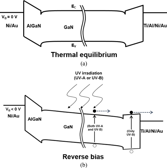
Schematic band diagrams of the fabricated MSM AlGaN UV sensor (a) at thermal equilibrium and (b) under reverse bias on the Ni/Au electrode.
The dark current density under a reverse bias of 2.0 V before dielectric breakdown was 1.2×10⁻⁸ A/cm2; however, this decreased to 1.1×10⁻⁹ A/cm2 owing to the surface passivation effect resulting from Joule heating due to dielectric breakdown. The relationship between the surface states of AlGaN and dark current was determined using XPS analysis, as described in Section 3.4.
3.2 Cross-sectional TEM images of the MSM AlGaN UV sensor before and after dielectric breakdown
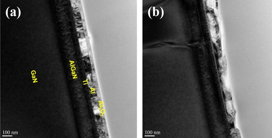
Fig. 5 shows cross-sectional TEM images taken near the Ti/Al/Ni/Au electrode region, which is the box area in Fig. 1(a), obtained before and after dielectric breakdown. In Fig. 5(a), the uniformity of the layers before dielectric breakdown is clearly visible, unlike that after dielectric breakdown, indicating that Joule heating caused interdiffusion between adjacent layers. Reports indicate that N2 and NH3 molecules are formed on the GaN surface owing to decomposition and reformation during the epitaxial growth of GaN in the temperature range of 600–1100 oC, leading to an N-segregated surface associated with VN [19-21]. In addition, N easily reacts with Ti to form TiN, and the remaining VN serves as a donor between AlGaN and the Ti/Al/Ni/Au electrode. The formation energy of VN was reported to be equivalent to shallow donor levels of 0.06 eV [22] and 0.25 eV [23] from the conduction band edge. Therefore, Joule heating due to dielectric breakdown was expected to generate temperatures over 600 oC, and the remaining VN in the AlGaN layer changed the contact behavior of the Ti/Al/Ni/Au electrode from Schottky to ohmic [25,26].
3.3 Spectral responsivity of the MSM Al0.24Ga0.76N UV sensor
Fig. 6 shows the spectral responsivity of the MSM AlGaN UV sensor before and after dielectric breakdown, with a cut-off wavelength of 316 nm obtained. The insets show the spectral responsivity under a forward bias. When the Ni/Au electrode was under forward bias, as shown in the inset of Fig. 6(a), spectral responsivity was observed, attributed to the low-barrier Ti/Al/Ni/Au electrode. After dielectric breakdown, no spectral responsivity was observed, as shown in the inset of Fig. 6(b), because of the electron current supplied owing to the near-ohmic behavior of the Ti/Al/Ni/Au electrode.
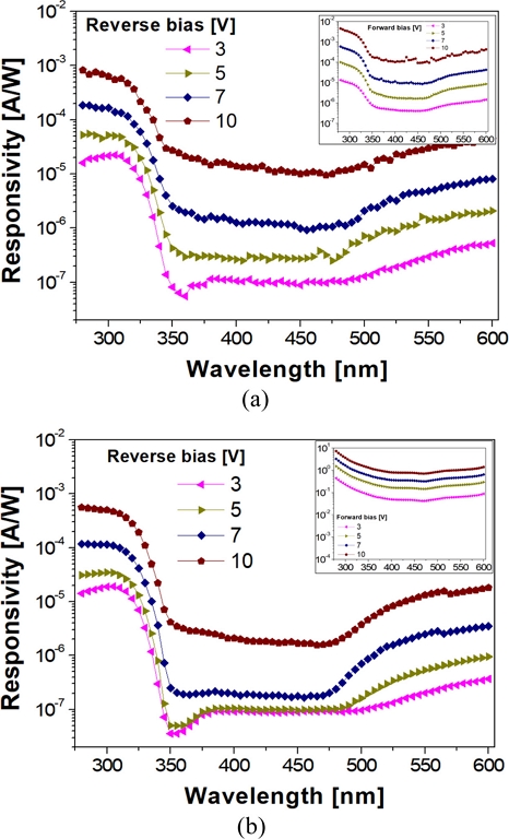
Spectral responsivity of the MSM AlGaN UV sensor (a) before and (b) after dielectric breakdown under a reverse bias. Insets show the spectral responsivity under forward bias.
Under a reverse bias of 7.0 V, the UVRR of the MSM AlGaN UV sensor before dielectric breakdown was 87, which significantly increased to 578, and a highly reliable responsivity was obtained. UVRR was calculated at 315 and 400 nm. Above 500 nm, the responsivity before and after dielectric breakdown was almost unchanged, attributed to bulk defects such as substitutional carbon (CN) acceptors and Ga vacancy hydrogen complexes (VGa-H complexes) [24]. The slight decrease of the responsivity as seen in Fig. 6(b) could be thermal effect of the annealing on the Schottky contact nearby.
3.4 XPS analysis
Fig. 7 shows the XPS spectrum of the MSMS-AlGaN UV sensor. The AlGaN sample used to obtain the graphs in Fig. 7(a) was etched across the AlGaN surface for 165 sec (40 nm) using an Ar ion gun at 500 eV, with O 1s spectra recorded every 5 sec. In this study, the O 1s spectrum was analyzed between 140 and 160 sec, during which the AlGaN surface was exposed. During fabrication, the quality of the AlGaN surface is affected owing to atmospheric oxidation, PR coating, lift-off, dry etching, and ashing. The Ga on the AlGaN surface reacts with atmospheric oxygen to form thin Ga-oxide layers, such as layers of unstable Ga2O and GaO2. These chemical bonds act as electron traps on the surface, providing a path for surface current leakage. In Fig. 7(b), the main peak in the O 1s spectrum is at 531.6 eV, corresponding to the Ga–O bond [27]. After dielectric breakdown, the intensity of O 1s decreased considerably from 822 to 691 counts/s before dielectric breakdown, indicating a reduction in the number of Ga–O bonds distributed on the AlGaN surface.
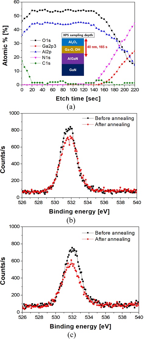
XPS analysis of the MSM AlGaN UV sensor: (a) at.% as a function of etch time, (b) O 1s XPS spectra associated with the Ga–O bond on the AlGaN surface, and (c) O 1s XPS spectra associated with OH- on the AlGaN surface of the MSM AlGaN UV sensor before and after dielectric breakdown.
Fig. 7(c) shows the O 1s XPS profiles of OH- on the AlGaN surface before and after dielectric breakdown. The peak in the O 1s spectrum appeared at 532.3 eV. Reports indicate that OH- is formed when AlGaN is exposed to air and acts as a surface-trapping state to capture electrons injected from the metal under reverse bias [28]. After dielectric breakdown, the intensity of the O 1s peak associated with OH- was 518, significantly lower than that before dielectric breakdown (724).
4. CONCLUSIONS
An asymmetric MSM Al0.24Ga0.76N UV sensor fabricated by dielectric breakdown was used to investigate the effects of local Joule heating on photoresponse characteristics. At a forward bias of 4.0 V under dark conditions, the current density after dielectric breakdown was 0.8 A/cm2, indicating a drastic increase from 3.0×10⁻⁵ A/cm2 before dielectric breakdown. The formation of VN due to local Joule heating caused by dielectric breakdown was responsible for the Schottky behavior of the Ti/Al/Ni/Au electrode changing to near-ohmic behavior. At a reverse bias of 2.0 V, the dark current density after dielectric breakdown was 1.1×10⁻⁹ A/cm2, lower than 1.2×10⁻⁸ A/cm2 before dielectric breakdown. The UVRR under a reverse bias of 7.0 V before dielectric breakdown was 87. After dielectric breakdown, the UVRR significantly increased to 578, in addition to providing highly reliable responsivity. XPS analysis of the AlGaN surface revealed that the peak intensities of the O 1s binding energies associated with Ga–O and OH-, which act as surface electron-trapping states on the AlGaN surface, were significantly decreased. These results demonstrate a remarkable improvement in the photoresponse performance without requiring additional fabrication processes and equipment. Thus, the proposed local heating method is expected to improve the sensing performance of UV optoelectronic integration devices such as active-pixel UV image sensors.
Acknowledgments
This study was supported by the National Research Foundation of Korea (NRF) grant funded by the Korean Government (No.2020R1I1A3A04037962). This work was also supported by the BK21 Four Project, funded by the Ministry of Education, Korea (No. 4199990113966).
REFERENCES
-
G. Wang, H. Lu, D. Chen, F. Ren, R. Zhang, and Y. Zheng, “High Quantum Efficiency GaN-Based p-i-n Ultraviolet Photodetectors Prepared on Patterned Sapphire Substrates”, IEEE Photon. Technol. Lett., Vol. 25, No. 7, pp. 652-654, 2013.
[https://doi.org/10.1109/LPT.2013.2248056]

-
Q. Cai, H. You, J. Wang, B. Liu, Z. Xie, D. Chen, H. Lu, Y. Zheng, and R. Zhang, “Progress on AlGaN-based solar-blind ultraviolet photodetectors and focal plane arrays”, Light Sci. Appl., Vol. 10, No. 94, pp. 1-31, 2021.
[https://doi.org/10.1038/s41377-021-00527-4]

-
Ö. Mikael, “High power device in wide bandgap semiconductors”, Sci. China Inf. Sci., Vol. 52, No. 5, pp. 1087-1093, 2011.
[https://doi.org/10.1007/s11432-011-4232-9]

-
N. Nasiri, D. Jin, and A. Tricoli, “Nanoarchitechtonics of Visible-Blind Ultraviolet Photodetector Materials: Critical Features and Nano-Microfabrication”, Adv. Opt. Mater., Vol. 7, No. 2, p. 1800580, 2019.
[https://doi.org/10.1002/adom.201800580]

-
J. Grant, R. Bates, W. Cunningham, A. Blue, J. Melone, F. McEwan, J. Vaitkus, E. Gaubas, and V. O’Shea, “GaN as a radiation hard particle detector”, Prog. Part. Nucl. Phys., Vol. 576, No. 1, pp. 60-65, 2007.
[https://doi.org/10.1016/j.nima.2007.01.121]

-
H. Y. Liu, W. C. Hsu, B. Y. Chou, and Y. H. Wang, “A Simple Passivation Technique for AlGaN/GaN Ultraviolet Schottky Barrier Photodetector”, IEEE Photon. Technol. Lett., Vol. 26, No. 2, pp. 138-141, 2014.
[https://doi.org/10.1109/LPT.2013.2290130]

-
H. Tian, B. Fowler, and A. E. Gamaml, “Anaylsis of Temporal Noise in CMOS Photodiode Active Pixel Sensor”, IEEE J. Solid-State Circuits, Vol. 36, No. 1, pp. 92-101, 2001.
[https://doi.org/10.1109/4.896233]

-
I. Brouk, A. Nemirovsky, and Y. Nemirovsky, “Analysis of Noise in CMOS Image Sensor”, Proc. of 2008 IEEE International Conference on Microwaves, Communications, Antennas and Electronic Systems, pp. 1-8, Tel-Aviv, Israel, 2008.
[https://doi.org/10.1109/COMCAS.2008.4562800]

-
F. Xie, H. Lu, D. Chen, R. Zhang, and Y. Zheng, “GaN MSM photodetectors fabricated on bulk GaN with low dark-current and high UV/visible rejection ratio”, Phys. Stat. Sol., Vol. 8, No. 7-8, pp. 2473-2475, 2011.
[https://doi.org/10.1002/pssc.201000884]

-
B. Ren, M. Liao, M. Sumiya, J. Huang, L. Wang, Y. Koide, and L. Sang, “Vertical-Type Ni/GaN UV Photodetectors Fabricated on Free-Standing GaN Substrates”, MDPI Appl. Sci., Vol. 9, No. 14, pp. 2895(1)-2895(8), 2019.
[https://doi.org/10.3390/app9142895]

-
Q. Lyu, H. Jiang, X. Lu, and K. M. Lau, “High Responsivity and Low Dark Current Ultraviolet Photodetectors Using p-GaN/AlGaN/GaN Heterostructure”, Proc. of Compound Semiconductor Week 2019, pp. 1-2, Nara, Japan, 2019.
[https://doi.org/10.1109/ICIPRM.2019.8819330]

-
C. J. Lee, Y. J. Kwon, C. H. Won, J. H. Lee, and S. H. Hahm, “Dual-wavelength sensitive AlGaN/GaN metalinsulator-semiconductor-insulator-metal ultraviolet sensor with balanced ultraviolet/visible rejection ratios”, Appl. Phys. Lett., Vol. 103, No. 11, p. 111110, 2013.
[https://doi.org/10.1063/1.4821133]

-
F. Xie, H. Lu, D. Chen, X. Ji, F. Yan, R. Zhang, Y. Zheng, L. Li, and J. Zhou, “Ultra-Low Dark Current AlGaN-Based Solar-Blind Metal-Semiconductor-Metal Photodetectors for High-Temperature Applications”, IEEE Sens. J., Vol. 12, No. 6, pp. 2086-2090, 2012.
[https://doi.org/10.1109/JSEN.2012.2184533]

-
J. Lee, D. Liu, H. Kim, and W. Lu, “Post-annealing effects on device performance of AlGaN/GaN HFETs”, Solid-State Electron., Vol. 48, No. 10-11, pp. 1855-1859, 2004.
[https://doi.org/10.1016/j.sse.2004.05.026]

-
B. P. Luther, S. E. Mohney, T. N. Jackson, M. A. Khan, Q. Chen, and J. W. Yang, “Investigation of the mechanism for Ohmic contact formation in Al and Ti/Al contacts to n-type GaN”, Appl. Phys. Lett., Vol. 70, No. 1, pp. 57-59, 1997.
[https://doi.org/10.1063/1.119305]

-
W. Lim, J. H. Jeong, J. H. Lee, S. B. Hur, J. K. Ryu, K. S. Kim, T. H. Kim, S. Y. Song, J. I. Yang, and S. J. Pearton, “Temperature dependence of current-voltage characteristics of Ni-AlGaN/GaN Schottky diodes”, Appl. Phys. Lett., Vol. 97, No. 24, p. 242103, 2010.
[https://doi.org/10.1063/1.3525931]

-
J. H. Seol and S. H. Hahm, “Selective Ohmic Contact Formation on Schottky Type AlGaN/GaN UV Sensors Using Local Breakdown”, IEEE Sens. J., Vol. 19, No. 8, pp. 2946-2949, 2019.
[https://doi.org/10.1109/JSEN.2019.2892556]

-
C. Zhao, N. Alfaraj, R. C. Subedi, J. W. Liang, A. A. Alatawi, A. A. Alhamoud, M. Ebaid, M. S. Alas, T. K. Ng, and B. S. Ooi, “Ⅲ-nitride nanowires on unconventional substrates: From materials to optoelectronic device applications”, Prog. Quantum. Electron., Vol. 61, pp. 1-31, 2018.
[https://doi.org/10.1016/j.pquantelec.2018.07.001]

-
C. Haller, J. F. Carlin, G. Jacopin, W. Liu, D. Martin, R. Butte, and N. Grandjean, “GaN surface as the source of non-radiative defects in InGaN/GaN quantum wells”, Appl. Phys. Lett, Vol. 113, No. 11, p. 111106, 2018.
[https://doi.org/10.1063/1.5048010]

-
A. Rebey, T. Boufaden, and B. E. Jani, “In situ optical monitoring of the decomposition of GaN thin films”, J. Cryst. Growth, Vol. 203, No. 1-2, pp. 12-17, 1999.
[https://doi.org/10.1016/S0022-0248(99)00081-0]

-
D. D. Koleske, A. E. Wickenden, R. L. Henry, J. C. Culbertson, and M. E. Twigg, “GaN decomposition in H2 and N2 MOVPE temperatures and pressures”, J. Cryst. Growth, Vol. 223, No. 4, pp. 466-483, 2001.
[https://doi.org/10.1016/S0022-0248(01)00617-0]

-
D. C. Look, “Defect-Related Donors, Acceptors, and Traps in GaN”, Phys. Stat. Sol., Vol. 228, No. 1, pp. 293-302, 2001.
[https://doi.org/10.1002/1521-3951(200111)228:1<293::AID-PSSB293>3.0.CO;2-F]

-
Z. Zhang, A. R. Arehart, E. Cinlilic, J. Chen, E. X. Zhang, D. M. Fleetwood, R. D. Schrimpf, B. McSkimming, J. S. Speck, and S. A. Ringel, “Impact of proton irradiation on deep level states in n-GaN”, Appl. Phys. Lett., Vol. 103, No. 4, pp. 042102(1)-042102(6), 2013.
[https://doi.org/10.1063/1.4816423]

-
M. A. Reshchikov, “On the Origin of the Yellow Luminescence Band in GaN”, Phys. Stat. Sol., Vol. 260, No. 8, pp. 2200488(1)-2200488(16), 2023.
[https://doi.org/10.1002/pssb.202200488]

-
T. Hashizume, J. Kotani, A. Basile, and M. Kaneko, “Surface Control Process of AlGaN for Suppression of Gate Leakage Currents in AlGaN/GaN Heterostructure Field Effect Transistor”, J. J. Appl. Phys., Vol. 45, No. 4. pp. L111-L113, 2006.
[https://doi.org/10.1143/JJAP.45.L111]

-
T. Hashizume, and H. Hasegawa, “Effects of nitrogen deficiency on electronic properties of AlGaN surfaces subjected to thermal and plasma processes”, Appl. Surf. Sci, Vol. 234, No. 1-4. pp. 387-394, 2004.
[https://doi.org/10.1016/j.apsusc.2004.05.091]

-
K. Makiyama, T. Ohki, N. Okamoto, M. Kanamura, S. Masuda, Y. Nakasha, K. Joshin, K. Imanishi, N. Hara, S. Ozaki, N. Nakamura, and T. Kikkawa, “High-Power GaN-HEMT with low current collapse for millimeter-wave amplifier”, Phys. Stat. Sol., Vol. 8, No. 7-8, pp.2442-2444, 2011.
[https://doi.org/10.1002/pssc.201001034]

-
F. Gao, Di Chen, H. L. Tuller, C. V. Thompson, and T. Palacios, “On the redox origin of surface trapping in AlGaN/GaN high electron mobility transistors”, J. Appl. Phys., Vol. 115, No. 12. p.124506, 2014.
[https://doi.org/10.1063/1.4869738]

