Area- and Energy-Efficient Ternary D Flip-Flop Design
This is an Open Access article distributed under the terms of the Creative Commons Attribution Non-Commercial License(https://creativecommons.org/licenses/by-nc/3.0/) which permits unrestricted non-commercial use, distribution, and reproduction in any medium, provided the original work is properly cited.
Abstract
In this study, we propose a ternary D flip-flop using tristate ternary inverters for an energy-efficient ternary circuit design of sequential logic. The tristate ternary inverter is designed by adding the functionality of the transmission gate to a standard ternary inverter without an additional transistor. The proposed flip-flop uses 18.18% fewer transistors than conventional flip-flops do. To verify the advancement of the proposed circuit, we conducted an HSPICE simulation with CMOS 28 nm technology and 0.9 V supply voltage. The simulation results demonstrate that the proposed flip-flop is better than the conventional flip-flop in terms of energy efficiency. The power consumption and worst delay are improved by 11.34% and 28.22%, respectively. The power–delay product improved by 36.35%. The above simulation results show that the proposed design can expand the Pareto frontier of a ternary flip-flop in terms of energy consumption. We expect that the proposed ternary flip-flop will contribute to the development of energy-efficient sensor systems, such as ternary successive approximation register analog-to-digital converters.
Keywords:
Sensors, ADC, Ternary logic circuits, Flip-flop1. INTRODUCTION
Sensor interfaces essentially require analog-to-digital converters (ADCs) to convert analog signals from the external environment to digital signals [1-3]. The advancement in integrated circuit (IC) technology demands lower power consumption and increased speeds for ADCs. Successive approximation register (SAR) ADCs are popular choices for low-power systems owing to their outstanding energy efficiency [4]. However, the capacitors used in SAR ADCs have limitations in both the area and speed [5].
Ternary logic has been applied to SAR ADCs to overcome these limitations in previous studies. Guerber et al. [6] proposed a ternary SAR ADC using quantization time information. This structure achieved improvements in operation speed and power reduction. However, the above structure requires additional circuits to use the time information. Reddy et al. [7] designed a ternary SAR ADC aimed at reducing the power consumption of comparators, thereby achieving an efficient area and power. However, the structure is limited by its slow operation speed owing to the doubling of the conversion phase.
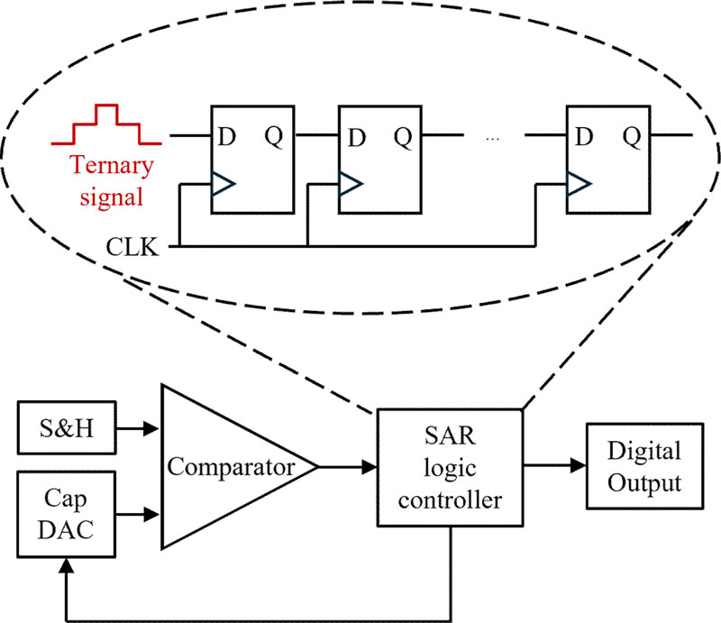
The two ternary SAR ADCs mentioned above used binary signals to represent the ternary values. Ternary logic requires less logic in gates and interconnect wires than binary logic [8]. Therefore, in ternary SAR ADCs, the use of a complete ternary signal is more efficient than using a binary signal. In addition, no attempts have been made to advance ternary SAR logic controllers. As a significant element of sequential logic, a flip-flop is used in the state machine of the SAR logic controller (Fig. 1). Therefore, improving ternary flip-flops can overcome the limitations of ternary ADCs.
Various attempts have been made to design ternary flip-flops using devices with adjustable threshold voltages. Sandhie et al. [9] proposed a ternary D flip-flop using graphene nanoribbon field effect transistors. This design comprised two D latches connected back-to-back. However, because one of the blocks constituting the D latch is a ternary NAND gate, many transistors were required. Moaiyeri et al. [10] proposed a ternary flip-flop based on carbon nanotube FET as components of a serial adder. Since the flip-flop, which was composed of standard ternary inverters (STIs), operated with the same supply voltage as the full adder, the additional voltage was not required. However, using an STI with a transmission gate (TG) required a relatively large number of transistors compared to the binary logic system.
In this study, we propose a new ternary flip-flop based on multithreshold CMOS (MTCMOS). This design utilizes a tristate ternary inverter (TTI) gate that combines the STI and TG, which are commonly used in ternary circuits. Therefore, the required number of transistors decreased by 18.18%, the power consumption decreased by 11.34%, and the worst delay decreased by 28.22%. The main contributions of this study are as follows:
- ㆍWe propose a tristate ternary inverter designed by adding the functionality of a transmission gate to a standard ternary inverter.
- ㆍWe designed a ternary flip-flop using a tristate ternary inverter.
- ㆍWe demonstrated that the proposed design is improved in terms of the energy efficiency and metastability window compared with the conventional ternary flip-flop.
The remaining content of this paper is organized as follows. Section 2 presents the proposed ternary D flip-flop. Section 3 describes the improvements in the area and power of the designed D flip-flop. Finally, section 4 concludes the paper.
2. PROPOSED DESIGN
Fig. 2 (a) shows three types of MTCMOS with different threshold voltages. Black represents the high-voltage threshold (HVT), the striped pattern is the regular voltage threshold (RVT), and white represents the super-low voltage threshold (SLVT). Fig. 2 (b) shows the truth tables for the inverter (INV), TG, and STI. Ternary logic values correspond to specific voltage levels: “0,” “1,” and “2” represent the “VDD,” “VDD/2,” and “Gnd” states, respectively.
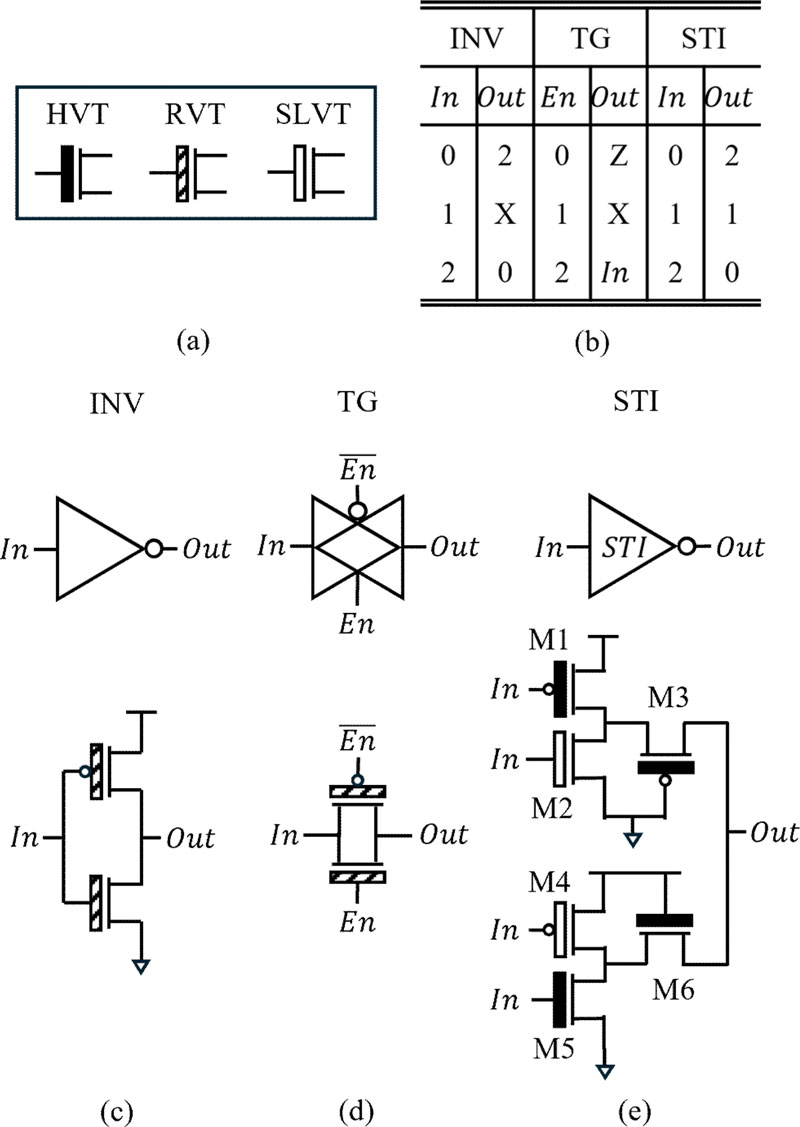
(a) Three types of MTCMOS with various threshold voltages. (b) Truth table for logic gates. Transistor-level schematic of logic gates: (c) inverter, (d) transmission gate, and (e) standard ternary inverter
Figs. 2 (c), 2 (d), and 2 (e) show schematics of the logic gates used in the proposed design: INV, TG, and STI, respectively. In Fig. 2 (c), INV was employed to drive the enable signal of the TG. In Fig. 2 (d), the TG was constructed by connecting the nMOS and pMOS in parallel. When the enable signal was 2, the TG could create a path from the input to the output. In Fig. 2 (e), the operation of the STI is detailed as follows: When the input value was “0,” both M1 and M4 were turned on. Hence, the output value was “2.” When the input value was “2,” both M2 and M5 were turned on. Hence, the output value was “0.” When the input value was “1,” both M2 and M4 were turned on. Hence, the output value was “1.” M3 and M6 were always turned on.
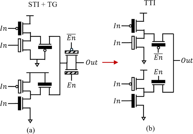
Figs. 3 (a) and 3 (b) show schematics of the STI with the TG and TTI gates. In Fig. 3 (b), the TTI gate was designed by eliminating the TG and reconnecting the enable signal, which formerly controlled the TG, to drive the pass transistor connected to the output of the STI. In other words, the TTI gate was designed by adding the functionality of the TG to the STI.
There are two main cases for the operation of the TTI gate depending on the level of the enable signal. When the enable signal was “0,” the pass transistor was turned off, and the output was placed in the z-state. However, if the enable signal value is “1,” the pass transistor is switched on, and the inverted value from the input is exported as the output.
Consequently, because the TTI gate had the same transistor count as the STI, the TTI gate operated equivalently to using STI and TG together in the flip-flop design, with a 25% reduction in transistor count. In addition, not all pass transistors in the STI were constantly turned on; instead, only one of them was switched on, depending on the enable signal. Therefore, the TTI gate could operate with a low power consumption.
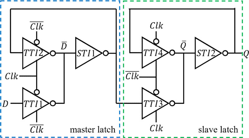
Fig. 4 shows a schematic of the proposed ternary D flip-flop. The master and slave latches are connected back-to-back by the TTI and STI, respectively, whereas the TG regulates the transfer of data between them. The TTI located at the input and STI located at the output contribute to the preservation of modularity. This method is useful to avoid unexpected interactions [11].
The operation of the proposed flip-flop can be divided into two states: (1) capturing a digital value within the circuit and (2) propagating the captured digital value to the STI connected to the output node.
(1) When logic values are captured in a circuit, the enable signal is 0, and TTI1 is activated. Hence, the input data are passed to, where the TTI and STI are connected back-to-back. When TTI2 is turned off, the back-to-back loop is broken, and the data remains in the master latch. Because TTI3 is turned off, the master and slave latches are separated. When TTI4 is turned on, the output node value remains unchanged.
(2) When the captured value is propagated to the STI of the output, the enable signal is 1. TTI1 is turned off. Thus, the input data are blocked from being passed back-to-back. TTI2 is turned on to connect the back-to-back loop. When TTI3 is activated, the data are transferred from the master latch to the slave latch. When TTI4 is turned off, the input data value is transferred to the output node.
3. RESULTS AND DISCUSSIONS
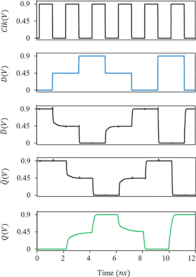
To analyze the characteristics of the proposed ternary flip-flop, we conducted a Synopsys HSPICE simulation with a CMOS 28 nm library. To prove the improvement in our research, we designed a conventional ternary flip-flop with MTCMOS based on an optimal gate design methodology [12]. We used six types of input signals that could demonstrate all the transitions in ternary logic to evaluate the function of the ternary flip-flop. The proposed design used four STIs as fan outs. We set the transient time to 0.01 ns and supplied a voltage of 0.9 V. Our report includes information on the average power consumption, worst clock-to-Q delay, setup time, hold time, and metastability window. We also computed the power–delay product (PDP) by multiplying the worst time delay by the average power.
The operation of the ternary flip-flop in response to an input set containing all transitions in the ternary logic is shown in Fig. 5. Because the output signal Q correctly followed the input signal D, we verified that the flip-flop successfully captured ternary values.
According to Table 1, the number of transistors used in the proposed flip-flop decreased by 18.18% compared with the previous design. Because of the reduced number of transistors, the average power consumption improved by 11.34%. The worst delay, measured as clock-to-Q, improved by 36.65% compared with the conventional design. We calculated the PDP by multiplying the average power consumption by the worst delay. The proposed design showed a 36.35% improvement in the PDP compared to the previous ternary flip-flop design. Based on the above results, the proposed design surpasses the conventional design in terms of average power consumption, worst delay, and PDP.
The setup and hold times were measured by adjusting the timing of the input signals. The setup time was 123 ps, and the hold time was 21 ps, showing improvements of 38.19% and 44.74%, respectively, over the conventional flip-flop. The metastability window, which indicates the timing width of an unstable data transition [13], was calculated as the sum of the setup and hold times, showing an improvement of 36.65% compared with the conventional design.
4. CONCLUSION
We presented a new ternary D flip-flop using a TTI gate. The TTI gate was designed by combining a standard ternary inverter with a transmission gate. We demonstrated that the proposed ternary flip-flop is more advanced than the conventional flip-flop in terms of energy consumption. Because of the reduction in the number of transistors, both the average power consumption and worst-delay time were improved.
Because we designed the proposed flip-flop using MTCMOS devices based on the ternary-logic synthesis methodology, it can be replaced by various devices that are applicable to ternary circuits. In addition, the power efficiency and performance can be improved if the size is optimized. We expect that the presented flip-flop will contribute to accomplishment of our following research on ternary SAR ADC using complete ternary signals and achieve high energy efficiency in the sensor system.
Acknowledgments
This research was supported by the Nanomaterials Development Program through the National Research Foundation of Korea (NRF) (2022M3H4A1A04096496), funded by the Ministry of Science and ICT, Korea.
REFERENCES
-
P. Harpe, Y. Shen, H. Li, K. Pelzers, H. Xin, and E. Cantatore, “Ultra Low Power Event-Driven Sensor Interfaces”, Proc. of 2023 9th International Workshop on Advances in Sensors and Interfaces (IWASI), pp. 133-137, Monopoli (Bari), Italy, 2023.
[https://doi.org/10.1109/IWASI58316.2023.10164620]

-
Y. Chae, C. M. Lopez, K. A. A. Makinwa, M. Ortmanns, and W. Sansen, “A Glimpse of the History of Analog ICs: A Tale of Amplifiers, Data Converters, and Sensor Interfaces”, IEEE Solid-State Circuits Magazine, Vol. 15, No. 3, pp. 43-52, 2023.
[https://doi.org/10.1109/MSSC.2023.3282557]

-
M. Ren, H. Xu, C. Dong, and Z. Zhang, “Toward a Gas Sensor Interface Circuit-A Review,” IEEE Sens. J., Vol. 22, No. 19, pp. 18253-18265, 2022.
[https://doi.org/10.1109/JSEN.2022.3199254]

-
R. Wang, “A Review on the Key Optimization Techniques of SAR ADC Design”, Proc. of 2021 International Conference on Electronic Information Engineering and Computer Science (EIECS), pp. 951-957, Changchun, China, 2021.
[https://doi.org/10.1109/EIECS53707.2021.9587905]

-
H. Wang, S. Wang, Y. Yuan, and G. Zhang, “Low power consumption and low area capacitor array for 16-bit 1-MS/ s SAR ADC”, Proc. of 2018 IEEE 3rd Advanced Information Technology, Electronic and Automation Control Conference (IAEAC), pp. 1003-1006, Chongqing, China, 2018.
[https://doi.org/10.1109/IAEAC.2018.8577797]

-
J. Guerber, H. Venkatram, M. Gande, A. Waters, and U. -K. Moon, “A 10-b Ternary SAR ADC With Quantization Time Information Utilization”, IEEE J. Solid-State Circuits, Vol. 47, No. 11, pp. 2604-2613, 2012.
[https://doi.org/10.1109/JSSC.2012.2211696]

-
Y. S. G. Reddy and Y. Y. H. Lam, “A low-power and areaefficient radix-3 SAR ADC”, Proc. of 2015 IEEE International Conference on Electron Devices and Solid-State Circuits (EDSSC), pp. 146-149, Singapore, 2015.
[https://doi.org/10.1109/EDSSC.2015.7285071]

-
S. Kim, S.-Y. Lee, S. Park, and S. Kang, “Design of Quad- Edge-Triggered Sequential Logic Circuits for Ternary Logic”, Proc. of 2019 IEEE 49th International Symposium on Multiple-Valued Logic (ISMVL), pp. 37-42, Fredericton, Canada, 2019.
[https://doi.org/10.1109/ISMVL.2019.00015]

-
Z. T. Sandhie, F. U. Ahmed, and M. H. Chowdhury, “Design of Ternary Master-Slave D-Flip Flop using MOSGNRFET”, Proc. of 2020 IEEE 63rd International Midwest Symposium on Circuits and Systems (MWSCAS), pp. 554-557, Springfield, USA, 2020.
[https://doi.org/10.1109/MWSCAS48704.2020.9184618]

-
M. H. Moaiyeri, M. Nasiri, and N. Khastoo, “An efficient ternary serial adder based on carbon nanotube FETs”, Eng. Sci. Technol. Int. J., Vol. 19, No. 1, pp. 271-278, 2016.
[https://doi.org/10.1016/j.jestch.2015.07.015]

- N. H. E. Weste and D. M. Harris, Principles of CMOS VLSI Design-A Circuits and Systems Perspective, 4th Edition Addison, Boston, Addison-Wesley, US, pp. 17-31, 2010.
-
S. Kim, S.-Y. Lee, S. Park, K. R. Kim, and S. Kang, “A Logic Synthesis Methodology for Low-Power Ternary Logic Circuits”, IEEE Trans. Circuits. Syst. I Regul. Pap., Vol. 67, No. 9, pp. 3138-3151, 2020.
[https://doi.org/10.1109/TCSI.2020.2990748]

- D. Li, P. Chuang, and M. Sachdev, “Comparative analysis and study of metastability on high-performance flip-flops”, Proc. of 2010 11th International Symposium on Quality Electronic Design, pp. 853-860, San Jose, USA, 2010.
