Energy-Efficient Ternary Modulator for Wireless Sensor Networks
This is an Open Access article distributed under the terms of the Creative Commons Attribution Non-Commercial License(https://creativecommons.org/licenses/by-nc/3.0/) which permits unrestricted non-commercial use, distribution, and reproduction in any medium, provided the original work is properly cited.
Abstract
The importance of Wireless Sensor Networks is becoming more evident owing to their practical applications in various areas. However, the energy problem remains a critical barrier to the progress of WSNs. By reducing the energy consumed by the sensor nodes that constitute WSNs, the performance and lifespan of WSNs will be enhanced. In this study, we introduce an energy-efficient ternary modulator that employs multi-threshold CMOS for logic conversion. We optimized the design with a low-power ternary gate structure based on a pass transistor using the MTCMOS process. Our design uses 71.69% fewer transistors compared to the previous design. To demonstrate the improvements in our design, we conducted the HSPICE simulation using a CMOS 180 nm process with a 1.8V supply voltage. The simulation results show that the proposed ternary modulator is more energy-efficient than the previous modulator. Power-delay product, a benchmark for energy efficiency, is reduced by 97.19%. Furthermore, corner simulations demonstrate that our modulator is stable against PVT variations.
Keywords:
WSNs, MVL, PSK, MTCMOS, Energy-efficient, Ternary, Modulator1. INTRODUCTION
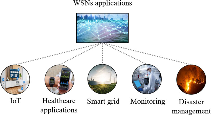
WSNs (Wireless Sensor Networks) are becoming increasingly important owing to their practical applications in various areas, as shown in Fig. 1 [1-5]. WSNs comprise sensor nodes and a network architecture. In these networks, sensor nodes are generally battery-powered, and the performance of these batteries directly affects the lifetime of the sensor network. Therefore, the power unit is an essential component, and energy issues are inevitable [6-7].
The total energy consumption of the entire network can be reduced by decreasing the energy usage of each sensor node. Several studies have been conducted to address this issue; however, most transmission standards in related research are based on binary transmission [8-12]. A recent study has suggested that a quaternary transmission scheme provides a more energy-efficient solution than a binary transmission scheme [13].
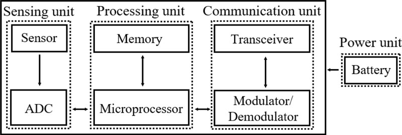
MVL (Multi-valued logic) data transmission consumes less power because fewer coded words will be used in data transmission [13]. Furthermore, MVL performs arithmetic operations faster than binary logic with fewer interconnections [14-15]. MVL systems can be realized using base three, base four, or other numeral bases. Ternary logic can be applied in phase shift keying (PSK). Modulator and demodulator are essential components to realize WSNs with PSK modulation as shown in Fig. 2. Baek et al. [16] proposed an energy-efficient ternary-to-binary (T2B) demodulator. Saha et al. [17] proposed a binary-to-ternary (B2T) modulator based on double pass-transistor Logic (DPL). However, owing to the structure of DPL circuits, where the logic gate must drive all the remaining parts, the previous modulator has weaknesses in energy efficiency. Kim et al. [18] proposed a logic synthesis methodology with a novel low-power circuit structure for ternary logic.
Optimizing the number of circuit elements and the power consumption in the modulator is vital in WSNs. This study proposes an energy-efficient 3-to-2 B2T modulator for the 8-ternary PSK, based on multi-threshold CMOS (MTCMOS). Our modulator converts 3-bit to 2-trit. Our design shows a significant improvement compared to previous design, demonstrating a remarkable decrease of 97.19% in the power-delay product (PDP) and a considerable reduction of 71.69% in device counts. The main contributions of this study are as follows.
- • An optimized B2T modulator is proposed with lower energy consumption, and reduced device counts compared with previous designs.
- • The existing low-power structure is optimized for ternary logic to integrate with MTCMOS.
- • The application of MVL data transmission is presented by applying ternary logic to PSK modulation.
The remainder of this paper is structured as follows. Section 2 presents the design of 3-to-2 B2T modulator for 8-ternary PSK. In Section 3, the simulation results of our design and the comparison with previous design are presented. Finally, section 4 presents the conclusions of the study.
2. PROPOSED DESIGN
We propose the design of 3-to-2 B2T modulator for 8-ternary PSK as shown in Fig. 3 (a). In 8-ternary PSK, two trits are used, which represent the phase. Fig. 3 (b) represents an 8-ternary PSK constellation plot. The plot is configured in a circular arrangement. Each point on the plot corresponds to one of the eight distinct phase states evenly spaced around the circle. These states were separated by 45°, as determined by dividing the full 360° circle by eight.
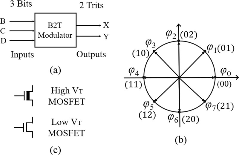
(a) 3-to-2 B2T modulator for 8-ternary PSK, (b) Constellation plot for 8-ternary PSK, (c) Thick-Tox MOSFET and thin-Tox MOSFET.
The main difference between the binary and ternary domains is the number of logic values. The binary domain uses two logic values. It represents ‘1’ as a VDD state (1.8 V) and ‘0’ as a GND state (0 V). The ternary domain uses the following three logical values. It represents ‘2’ as a VDD state (1.8 V), ‘1’ as a VDD/2 state (0.9 V), and ‘0’ as a GND state (0 V). We use MTCMOS to represent these states. To implement the multi-threshold voltage, we use two different oxide thicknesses Tox (i.e., thick-Tox and thin-Tox), as shown in Fig. 3 (c). The thick-Tox MOSFET has a high threshold voltage (VT) and is therefore turned off when the gate voltage is in the VDD/2 state. In contrast, the thin-Tox MOSFET has low VT and, therefore, turns on when the gate voltage is at VDD/2 state.
The primary function of the B2T modulator is to represent the VDD/2 state. To realize this function, we create two signal paths as shown in Fig. 4 (a): the half VDD path and the VDD/GND path. Each path has pull-up and pull-down networks. On the half VDD path, the pull-up and pull-down networks are used to drive the output node to the VDD/2 state. In the VDD/GND path, the pull-up network drives the output node to the VDD state, whereas the pull-down network drives it to the GND state. We adopt the state-of-the-art design presented in [18], with pull-up and pull-down networks connected to the pass transistors to reduce power consumption. In pass transistors, threshold drop and body effect enable the energy-efficient design of ternary logic circuits by managing output voltage transition and retention [18]. A mid-Tox, medium oxide thickness, MOSFET is used as a pass transistor in [18]. In our design, the thick-Tox MOSFET, the key component for reducing the PDP, is used instead. This MOSFET has high VT. Therefore, the off-current required to retain the output voltage at VDD/2 is reduced, and the power consumption in the VDD/2 state is also reduced.
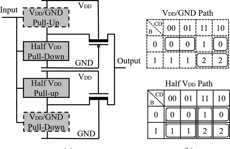
(a) Structure of the 3-to-2 B2T modulator with two signal paths. (b) Two K-maps of ternary output X in Table 1. (VDD/GND path K-map and Half VDD path K-map)
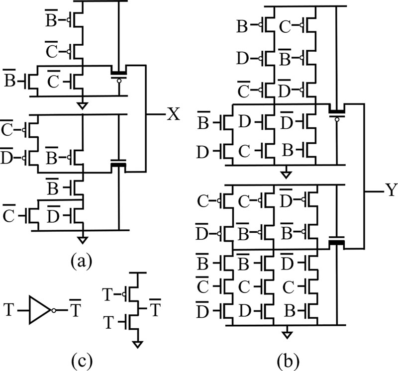
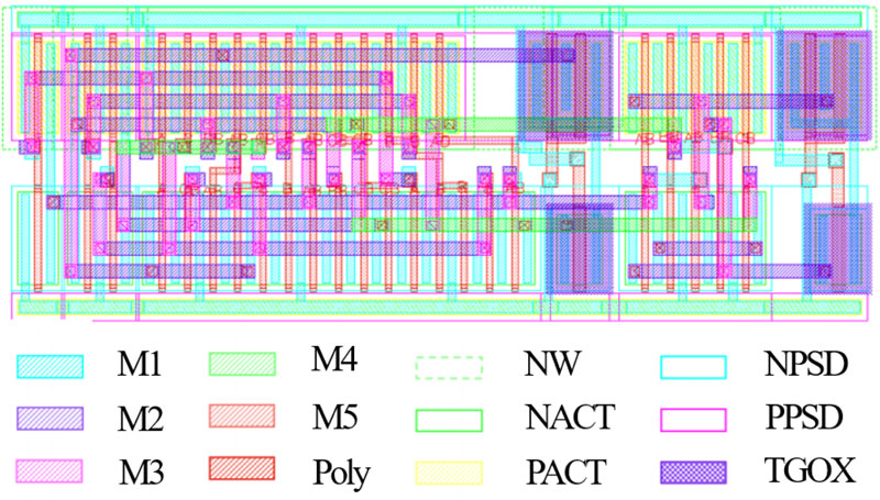
For the operation of 3-to-2 B2T modulator, we form a truth table as shown in Table 1. The truth table derives two different K-maps in Fig. 4 (b): the VDD/GND path K-map and the half VDD path K-map. Fig. 4 (b) shows two K-maps of the ternary output X in Table 1. Red boxes and blue boxes are represented in each K-map to construct the pull-up/pull-down network in Fig. 4 (a). The blue boxes represent the SOP terms of the pull-down networks, and the red boxes represent the SOP terms of the pull-up networks. The method of matching the transistors is same with binary static logic gates. Fig. 5 shows the transistor-level schematic of the 3-to-2 B2T modulator. Fig. 6 shows the layout of the 3-to-2 B2T modulator.
3. SIMULATION SETUP AND RESULTS
3.1 Simulation Setup
We use the CMOS 180 nm process with 1.8 V supply voltage. We design a schematic and layout of the modulator circuit, using the Cadence Virtuoso. We conduct Calibre DRC, LVS, and PEX. To obtain the circuit characteristics, we execute a post-layout simulation using Synopsys HSPICE with a parasitic RC. In the thin Tox MOSFET, the width was set to 2.64um with a length of 180 nm. Conversely, in the thick Tox MOSFET, the width was set to 2um with lengths of 300 nm for p-type MOSFET and 350 nm for n-type MOSFET. Transistor size tuning is required in some circuits for correct operation. Each input pattern, with a 10ns pulse width and 20ps transient time, is thoroughly verified. The load capacitance is 5f F. We demonstrate the stability of our modulator under variations through corner simulations using three model parameters, namely, TT, FF, and SS. We consider 10% voltage variation, including 1.8, 1.98, 1.62 V along with three temperatures of -40, 25, and 125oC.
3.2 Simulation Results
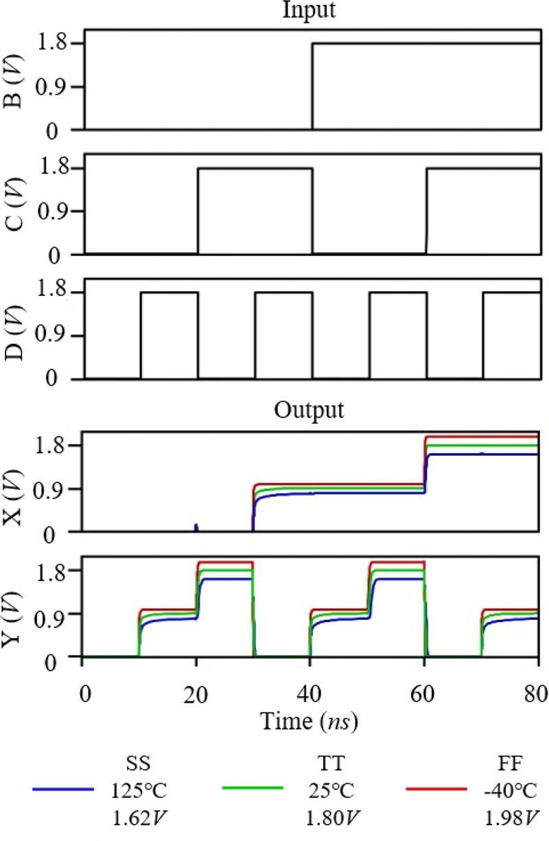
The waveform of the 3-to-2 B2T modulator is presented in Fig. 7, demonstrating that our design functions well and no data is lost during data conversion. The characteristics of the B2T modulator are listed in Table 2. We evaluated the design in [17] using self-implementation, and the results are listed in Table 3. Our design has smaller overheads in terms of power, delay, and area than the previous design. Corner simulations in our circuit demonstrate stability against PVT variations. Our design exhibits a reduction in PDP by 97.19% and in device counts by 71.69% compared to those with the previous design.
4. CONCLUSIONS
In this study, we proposed an energy-efficient 3-to-2 B2T modulator for 8-ternary PSK, based on MTCMOS. By replacing the mid-Tox MOSFET used as a pass transistor with thick-Tox MOSFET, we optimized the low-power ternary logic structure in [18] to integrate with MTCMOS. We proved that our modulator is more efficient than the previous modulator in terms of energy consumption. We reduced PDP by 97.19% and device counts by 71.69% with our current design compared with the previous design. Our design, exhibiting energy-efficient performance, is ideal for use in sensor node. By reducing the energy consumption in the sensor nodes that constitute WSNs, we expect that our modulator will enhance the performance and lifespan of WSNs. Our future work includes analyzing the comprehensive impact of applying our modulator in various wireless sensor network environments.
Acknowledgments
This study was supported by Kyungpook National University Research Fund, 2024.
REFERENCES
-
R. N. Gore, H. Kour, M. Gandhi, D. Tandur, and A. Varghese, “Bluetooth based Sensor Monitoring in Industrial IoT Plants”, Proc. of 2019 International Conference on Data Science and Communication (IconDSC), pp. 1-6, Bangalore, India, 2019.
[https://doi.org/10.1109/IconDSC.2019.8816906]

-
S. Srivastava and J. N. Singh, “Wireless Communication Security Breaches in Smart Healthcare Applications”, Proc. of 2021 3rd International Conference on Advances in Computing, Communication Control and Networking (ICAC3N), pp. 1240-1244, Greater Noida, India, 2021.
[https://doi.org/10.1109/ICAC3N53548.2021.9725738]

-
Y. Boloorchi and S. Azizi, “An IoT-Fog-Cloud Framework for Demand Side Management in Smart Grid”, Proc. of 2021 5th International Conference on Internet of Things and Applications (IoT), pp. 1-6, Isfahan, Iran, 2021.
[https://doi.org/10.1109/IoT52625.2021.9469712]

-
S. Abraham, J. Beard, and R. Manijacob, “Remote environmental monitoring using Internet of Things (IoT)”, Proc. of 2017 IEEE Global Humanitarian Technology Conference (GHTC), pp. 1-6, San Jose, USA, 2017.
[https://doi.org/10.1109/GHTC.2017.8239335]

-
F. Franchi, A. Marotta, C. Rinaldi, F. Graziosi, and L. D'Errico, “IoT-based Disaster Management System on 5G uRLLC Network”, Proc. of 2019 International Conference on Information and Communication Technologies for Disaster Management (ICT-DM), pp. 1-4, Paris, France, 2019.
[https://doi.org/10.1109/ICT-DM47966.2019.9032897]

-
H. Yetgin, K. T. K. Cheung, M. El-Hajjar, and L. H. Hanzo, “A Survey of Network Lifetime Maximization Techniques in Wireless Sensor Networks”, IEEE Commun. Surv. Tutor., Vol. 19, No. 2, pp. 828-854, 2017.
[https://doi.org/10.1109/COMST.2017.2650979]

-
V. P. Nighot, S. M. Lambor, and S. M. Joshi, “Efficient battery management in wireless sensor node: Review paper”, Proc. of 2014 Eleventh International Conference on Wireless and Optical Communications Networks (WOCN), pp. 1-5, Vijayawada, India, 2014.
[https://doi.org/10.1109/WOCN.2014.6923085]

-
V. Nagaraju, N. J. Kumar, A. M. Ali, T. B. R. Bapu, and N. Partheeban, “Efficient Data Transmission Scheme using Modified Wireless Communication Protocol Design”, Proc. of 2022 International Conference on Advances in Computing, Communication and Applied Informatics (ACCAI), pp. 1-7, Chennai, India, 2022.
[https://doi.org/10.1109/ACCAI53970.2022.9752622]

-
S. Alizadeh and A. Ghaffari, “An Energy-efficient hirerchical Clustering protocole in wireless sensor networks”, Proc. of 2010 3rd International Conference on Computer Science and Information Technology, pp. 413-418, Chengdu, China, 2010.
[https://doi.org/10.1109/ICCSIT.2010.5564754]

-
T. M. Behera, U. C. Samal, S. K. Mohapatra, M. S. Khan, B. Appasani, N. Bizon, and P. Thounthong, “Energy-Efficient Routing Protocols for Wireless Sensor Networks: Architectures, Strategies, and Performance”, Electronics, Vol. 11, No. 15, pp. 2282(1)-2282(26), 2022.
[https://doi.org/10.3390/electronics11152282]

-
G. Xiaowang and Z. Jianyong, “Analysis and design of energy-oriented security protocols for Wireless Sensor Networks”, Proc. of IEEE Conf. on Electronic & Mechanical Engineering and Information Technology, pp. 2298-2301, Harbin, China, 2011.
[https://doi.org/10.1109/EMEIT.2011.6023570]

-
Y. Zeng and L. Wang, “Energy-saving routing protocol for Wireless Sensor Networks”, Proc. of the 26th Chinese Control and Decision Conference (2014 CCDC), pp. 4868-4872, Changsha, China, 2014.
[https://doi.org/10.1109/CCDC.2014.6853045]

-
N. Saleh, A. Kassem, and A. M. Haidar, “Energy-Efficient Architecture for Wireless Sensor Networks in Healthcare Applications”, IEEE Access, Vol. 6, pp. 6478-6486, 2018
[https://doi.org/10.1109/ACCESS.2018.2789918]

-
B. S. Raghavan and V. S. K. Bhaaskaran, “Design of novel Multiple Valued Logic (MVL) circuits”, Proc. of 2017 International Conference on Nextgen Electronic Technologies: Silicon to Software (ICNETS2), pp. 371-378, Chennai, India, 2017.
[https://doi.org/10.1109/ICNETS2.2017.8067963]

-
S. Lin, Y. B. Kim, and F. Lombardi, “CNTFET-Based Design of Ternary Logic Gates and Arithmetic Circuits”, IEEE Trans. Nanotechnol., Vol. 10, No. 2, pp. 217-225, 2011.
[https://doi.org/10.1109/TNANO.2009.2036845]

-
S. Baek, S. Kim, Y. Choi, and S. Kang, “MTCMOS-based Ternary to Binary Converter”, Proc. of 2020 International SoC Design Conference (ISOCC), pp. 5-6, Yeosu, Korea (South), 2020.
[https://doi.org/10.1109/ISOCC50952.2020.9333078]

-
A. Saha and D. Pal, “DPL-based novel Binary-to-ternary converter on CMOS technology”, AEU-Int. J. Electron. Commun., Vol. 92, pp. 69-73, 2018.
[https://doi.org/10.1016/j.aeue.2018.05.020]

-
S. Kim, S. Y. Lee, S. Park, K. R. Kim, and S. Kang, “A Logic Synthesis Methodology for Low-Power Ternary Logic Circuits”, IEEE Trans. Circuits Syst. I Regul. Pap., Vol. 67, No. 9, pp. 3138-3151, 2020.
[https://doi.org/10.1109/TCSI.2020.2990748]

