Novel Design of 8T Ternary SRAM for Low Power Sensor System
This is an Open Access article distributed under the terms of the Creative Commons Attribution Non-Commercial License(https://creativecommons.org/licenses/by-nc/3.0/) which permits unrestricted non-commercial use, distribution, and reproduction in any medium, provided the original work is properly cited.
Abstract
In this study, we propose a novel 8T ternary SRAM that can process three logic values (0, 1, and 2) with only two additional transistors, compared with the conventional 6T binary SRAM. The circuit structure consists of positive and negative ternary inverters (PTI and NTI, respectively) with carbon-nanotube field-effect transistors, replacing conventional cross-coupled inverters. In logic ‘0’ or ‘2,’ the proposed SRAM cell operates the same way as conventional binary SRAM. For logic ‘1,’ it works differently as storage nodes on each side retain voltages of VDD/2 and VDD, respectively, using the subthreshold current of two additional transistors. By applying the ternary system, the data capacity increases exponentially as the number of cells increases compared with the 6T binary SRAM, and the proposed design has an 18.87% data density improvement. In addition, the Synopsys HSPICE simulation validates the reduction in static power consumption by 71.4% in the array system. In addition, the static noise margins are above 222 mV, ensuring the stability of the cell operation when VDD is set to 0.9 V.
Keywords:
Multivalued logic, CNTFET, SRAM, Ternary logic circuits1. INTRODUCTION
With the emergence of artificial intelligence (AI) and Internet of Things (IoT) technologies, the importance of SRAM has received recurrent attention [1-3]. SRAM is located close to the processor and is a critical solution to data bottlenecks owing to its fast data access. Additionally, because of its simple operating mode and mature technology, it has become a widely used memory device, not only in microprocessors but also in various applications. Among them, SRAM is applied to numerous sensor technologies, such as wearable devices, image processing, and wireless devices [4-6]. Because the latest technologies require large amounts of data, combining sensors with them requires a low-power system while maintaining a small form factor.
However, conventional binary SRAM, which uses six transistors per bit, has a large cell size compared with its data capacity. Despite ongoing efforts in device scaling, there remain limitations in processing significant amounts of data [7]. As a breakthrough, multivalued logic (MVL) can improve the data capacity compared with a binary system [8]. In digital circuits, a multidigit system can be used by dividing the voltage levels into more than high/low levels. As the first step in MVL logic development, three-valued (ternary) logic has been studied in various fields.
In particular, carbon nanotube field-effect transistors (CNTFET) have been studied for use in ternary-logic systems [9]. As transistor technology scales down, complementary metal-oxide-semiconductor (CMOS) technology faces limitations owing to its short-channel effects and leakage power dissipation [10,11]. By contrast, CNTFETs can be scaled down to a sub-10 nm dimension at room temperature through the ballistic transport of charge carriers. In addition, it is suitable for MVL because it is easy to modulate the threshold voltage by adjusting the chirality vector of the CNTs.
With the ternary-logic system, a memory device can represent three values in a single cell. The simplest approach to implementing a ternary SRAM is to connect two standard ternary inverters (STIs) and store data in their feedback loops. Research on the 14T ternary SRAM using CMOS-based 6T STIs is a representative example [12]. However, this approach is inefficient in terms of the number of transistors relative to the data capacity. The data capacities of the binary and ternary systems are 2n and 3n for n cells, respectively. Therefore, to process the same amount of data, ternary requires only approximately log32 ≈ 0.63× as many cells as binary. Simultaneously, 0.63×14/6 ≈ 1.47× transistors are needed, which implies more transistors are required to process the same data as shown in Fig. 1 (a).

(a) Data density of MVLs. (b) Schematics of PTI and NTI. (c) Schematic symbols and threshold voltage for LVT, RVT, and HVT of CNTFET
This paper proposes an 8T ternary SRAM cell based on the CNTFET technology [13,14]. This design requires only 0.63×8/6 ≈ 0.84 × transistors compared to binary, effectively increasing the data density. The power consumption of the entire system can also be reduced by using fewer cells to process the same data. Furthermore, the design reduces power consumption by utilizing a subthreshold current. We validated the functionality and performance using HSPICE simulations by comparing our design not only with the 6T binary SRAM but also with other ternary SRAM models [12,15]. This study makes three contributions.
- • Lowest transistor count among ternary SRAM designs
- • 18.87% data density improvement compared with 6T binary SRAM
- • 71.4% reduction in static power consumption compared with 6T binary SRAM.
2. EXPERIMENT
2.1 Preliminary
Among MVL systems, ternary logic is a numerical system with three logical values represented as (0, 1, 2) or (-1, 0, +1), known as unbalanced and balanced ternary logic, respectively. The three values indicate (GND, VDD/2, VDD). This study focuses on unbalanced ternary logic. Implementing a ternary logic state requires two distinct multi-threshold voltage values [8]; in our case, we employed a low threshold voltage (LVT) and high threshold voltage (HVT) without a regular threshold voltage (RVT) in the cell. Voltage values lower than the LVT correspond to logic ‘0,’ values higher than the HVT correspond to logic ‘2,’ and the voltage levels between these thresholds correspond to logic ‘1.’
To process the middle logic state ‘1’, other types of inverters exist. As shown in Fig. 1 (b), a positive ternary inverter (PTI) and a negative ternary inverter (NTI) are composed of two types of transistors. While receiving logic ‘0’ and ‘2’ as inputs, both inverters output the inverted values ‘2’ and ‘0’, respectively. However, when the input is logic ‘1’, PTI outputs ‘2’, and NTI outputs ‘0’.
CNTFET is a type of field-effect transistor that uses the carbon nanotube as a channel from the source to the drain [13,14]. Fig. 1 (c) shows schematics of MOSFET-like CNTFETs. They exhibit semiconducting or metallic properties based on the angle of atomic arrangement, known as the chirality vector, which is expressed as a pair of integers (n and m). The chirality vector not only determines the electronic properties but also influences the tube diameter and threshold voltage of the CNTFET. The relationship between the parameters can be defined using the following equation, where m = 0:
| (1) |
Typically, the n- and p-type CNTFETs employ three threshold voltages: LVT, RVT, and HVT. In this study, the chirality vectors were set as (17, 0), (13, 0), and (8, 0) for the respective thresholds. For the n-type CNTFETs, the corresponding values were 0.323, 0.428, and 0.687 V. The SRAM cell utilizes LVT and HVT, whereas the peripheral circuitry employed for operational verification uses all three types of transistors.
Conventional binary SRAM cells store 1 bit of data per cell, whereas ternary SRAM cells store 1 trit of data. Therefore, the amount of data that can be processed per n cells is 2n for binary and 3n for ternary systems, respectively. This implies that the data capacity of the ternary systems increases exponentially as the total array size increases. Conversely, when two types of logical systems process the same 2n data points, the number of cells required for the ternary system compared with the binary system can be expressed by the following equation:
| (2) |
To implement ternary SRAM cells, several studies have utilized the structure of cross-coupled inverters with various types of STIs. However, while conventional binary inverters consist of two transistors per bit, STIs require six or more transistors to implement one trit. Consequently, unlike binary SRAM, which employs only six transistors per cell, ternary SRAM cells require a significantly higher number of transistors. This leads to inefficiencies in the memory array density.
In [12], an SRAM trit cell with 14 transistors was designed based on 6T STIs with CMOS technology. However, to process 2n data points, a binary SRAM requires n cells, thereby necessitating 6n transistors. By contrast, ternary SRAM can only process n×log32 cells. Thus, it is effective when the number of transistors per cell is less than 6×log23 ≈ 9.51.
2.2 Proposed Design
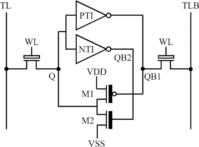
Conventional SRAMs store data in a symmetric feedback loop structure of cross-coupled inverters. However, in ternary systems, STIs require more than six transistors, resulting in transistor count overhead. Without conventional structures, an SRAM trit cell design implemented with only eight transistors based on CNTFETs was proposed in this study.
As shown in Fig. 2, it consists of PTI, NTI, and two additional transistors, M1 and M2, which form the structure of an asymmetric feedback loop. When the stored data of the Q node is ‘0’ or ‘2,’ it works the same as conventional SRAMs. This is because the same values are input to M1 and M2, which operate as general inverters. However, when the data are ‘1,’ PTI and NTI lead to differing inputs of ‘2’ and ‘0’ to M1 and M2, respectively, which results in both transistors turning off. Subsequently, the feedback loop continues to operate because of the subthreshold current.
This section describes the operations at VDD/2, including HOLD, READ, and WRITE. For the HOLD operation, it was assumed that the Q node retained a trit of '1'. When VDD/2 was applied to the inputs of PTI and NTI, the gate of the p-type M1 transistor received VDD, whereas the gate of the n-type M2 received GND. Subsequently, node Q maintained the logic state '1' through the subthreshold currents from each transistor, effectively sustaining this value through the feedback loop.
For the READ operation, the initial values of TL/TLB were forced to VDD/2 using a pre-charge circuit. The WL node, which was the gate of the access transistors, received VDD/2 instead of VDD. This prevented the flipping of the stored data ‘1’ corresponding to VDD/2 while the WL voltage was raised. When trit ‘1’ was stored at the Q node and ‘2’ at the QB1 node, both n-type access transistors remained turned off at VGS = 0 V and no potential change occurred at the TL/TLB nodes. Thus, the sense amplifier output VDD/2, which corresponded to ‘1’.
In WRITE, VDD was applied to the WL node. Assuming that '0' was initially stored before writing trit ‘1’, nodes Q and QB1 had voltages of GND and VDD, respectively. Because there was PTI between the data input terminal and TLB node inside the write driver, ‘1’ and ‘2’ were applied to the TL and TLB nodes, respectively. Consequently, the right access transistor turned off with VGS = 0V, whereas the left access transistor was activated, forcing the Q node to ‘1’. Consequently, through PTI and NTI in the cell, nodes QB1 and QB2 stored ‘2’ and ‘0’, respectively.
3. RESULTS AND DISCUSSION
3.1 Simulation Set-up
A 32 nm Stanford CNTFET model [13,14] was used to design the proposed 8T SRAM trit cell with a supply voltage of 0.9 V. The static noise margin (SNM) was assessed by altering the DC sweep voltage in increments of 1 mV to detect the flips. The power consumption and delay of the SRAM cells were measured via transient simulations using Synopsys HSPICE. The input transient time was set to 10 ps with rise and fall delays of 1 ps each, totaling 420 ns. Four STI gates were used as fanout loads for the transient simulations of the proposed design with full circuitry. For performance comparison, existing designs, including the 6T binary SRAM and 14T, 20T, and 24T ternary SRAM models, were also designed using the CNTFET and evaluated.
3.2 Performance Comparison
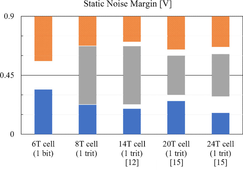
The SNM is an indicator of the amount of noise allowed in the input inside the cell to maintain a stable state [16]. The measured SNMs are shown in Fig. 3. Each bar graph represents the SNM values based on VDD, VDD/2, and GND. In the case of the 6T cell, the highest value was 341 mV for both VDD and GND, but it was based on 1 bit of data, and the area outside the margin was 218 mV. In the case of ternary SRAM cells, three logic values were distinguished based on the same power-supply voltage: the proposed 8T ternary SRAM design had the smallest area outside the margin, at a total of 6 mV. In addition, the noise margin values were 225, 222, and 225 mV, which had the smallest deviation among the three logic states. This indicated that the proposed design has the most stable tolerance to noise among the ternary SRAM models.
To evaluate the power and delay measurements, all the data changes were measured for each operation. The measured values were compared with those of other models using the average value. Table 1 lists the average power consumption values for each operation. The proposed 8T ternary SRAM consumed the lowest power among all the comparison models, and compared to the binary SRAM, it exhibited improved power efficiencies of 54.7%, 17.5%, and 34.6% for the HOLD, READ, and WRITE operations, respectively. Moreover, this result was the measurement of a single cell. For the same data, a ternary system uses a lower cell count than a binary system. Consequently, as the memory array expands, the percentage reduction in power consumption increases. The power consumption of the HOLD operation, which is the state of data storage, refers to the static power consumption. With cell reduction through ternary logic, the static power consumption can be reduced by 54.7×log32 ≈ 71.4% in the array system. Table 2 lists the average delay values for each operation. The proposed design had a slower speed than the binary SRAM. However, compared to other ternary SRAM models, it exhibited the lowest value in the READ operation and was also close to the fastest 20T cell in the WRITE operation.
3.3 Transient Simulations
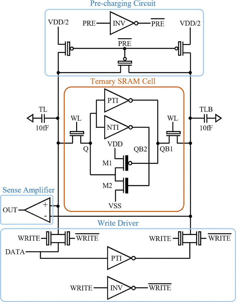
Peripheral circuits were designed to verify the functionality of the proposed ternary SRAM cell design, as shown in Fig. 4. The write driver enforced the TL/TLB nodes to align with the input data during the WRITE operation. The pre-charge circuit forced the TL/TLB nodes to VDD/2 to facilitate the READ operation. Finally, the sense amplifier received the potential from the TL/TLB nodes and delivered it to the output node based on the potential difference between the two inputs.
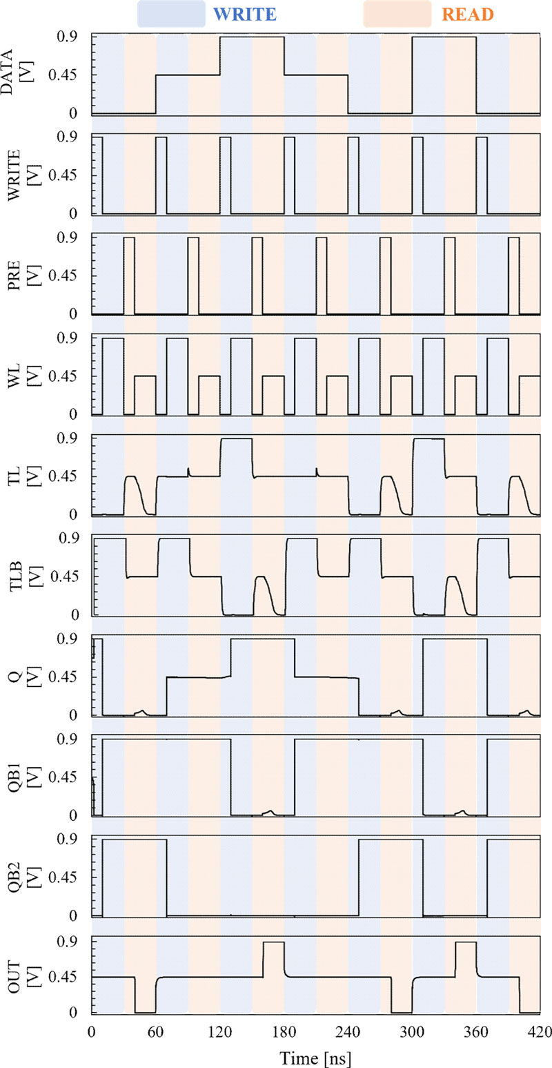
As shown in Fig. 5, the data were input in the sequence ‘0 → 1 → 2 → 1 → 0 → 2 → 0’, with WRITE and READ operations performed for each data value. This approach ensured the comprehensive testing of the functionality of the SRAM cell across its entire operational range. To write data 0, 1, or 2 to the Q node, the write driver was activated when the WRITE signal was turned on. After the TL and TLB nodes were charged to (0, 2), (1, 2), or (2, 0), these data were stored in the Q/QB1 node as soon as WL increased. In the READ scheme, the pre-charge circuit was activated when signal PRE was turned on, and both the TL and TLB nodes were set to VDD/2. After WL reached the middle (VDD/2), the potential of the TL/TLB nodes was discharged or maintained at (0, 1), (1, 1), or (1, 0), depending on the data stored in Q/QB1. The potential difference of the corresponding voltage-level pairs was detected through the sense amplifier and output to the OUT node as 0, 1, or 2.
4. CONCLUSIONS
This study demonstrated the feasibility of ternary SRAM for sensor systems with small form factors and large-scale data. A ternary SRAM design with eight transistors based on CNTFETs was proposed. PTI, NTI, and two additional transistors were applied to the proposed SRAM for an asymmetric feedback loop. The practical efficacy of the 8T SRAM trit cell was demonstrated by comparing its data density with those of other SRAM models. The measurement of SNMs ensures stability in ternary-logic systems. The simulation results demonstrated the power consumption and delay improvement of the proposed ternary SRAM compared with previous ternary SRAM designs. Additionally, the reduction in static power consumption was described in comparison with binary SRAM in a memory array system. For the proposed design, the cell operation was demonstrated by simulation with peripheral circuits. As future research, it is expected to develop a ternary in-memory computing system with high energy efficiency based on the proposed SRAM cell.
Acknowledgments
This research was supported by the Nanomaterials Development Program through the National Research Foundation of Korea (NRF) (2022M3H4A1A04096496) funded by the Ministry of Science and ICT, Korea.
REFERENCES
-
C. J. Jhang, C. X. Xue, J. M. Hung, F. C. Chang, and M. F. Chang, “Challenges and trends of SRAM-based computing-in-memory for AI edge devices”, IEEE Trans. Circuits Syst. I Regul. Pap., Vol. 68, No. 5, pp. 1773-1786, 2021.
[https://doi.org/10.1109/TCSI.2021.3064189]

-
J. Y. Kim, B. Kim, and T. T. H. Kim, Processing-in-Memory for AI, Springer, Cham, CH, pp. 1-165, 2022.
[https://doi.org/10.1007/978-3-030-98781-7_9]

-
H. N. Patel, F. B. Yahya, and B. H. Calhoun, “Optimizing SRAM bitcell reliability and energy for IoT applications”, Proc. of the 17th Int. Symp. Qual. Electron. Design, pp. 12-17, Santa Clara, CA, USA, 2016.
[https://doi.org/10.1109/ISQED.2016.7479149]

-
J. R. Dinesh Kumar, C. Ganesh Babu, V. R. Balaji, K. Priyadharsini, and S. P. Karthi, “Performance investigation of various SRAM cells for IoT based wearable biomedical devices”, Proc. of 5th International Conference Information, Communication & Computing Technology (ICICCT- 2020), pp. 573-588, New Delhi, India, 2021.
[https://doi.org/10.1007/978-981-15-7345-3_49]

-
V. Sharma, S. Vishvakarma, S. S. Chouhan, and K. Halonen, “A write?improved low?power 12T SRAM cell for wearable wireless sensor nodes”, Int. J. Circuit Theory Appl., Vol. 46, No. 12, pp. 2314-2333, 2018.
[https://doi.org/10.1002/cta.2555]

-
H. Lam, F. Guo, H. Qiu, M. Zhang, H. Jiao, and S. Zhang, “Pseudo multi-port SRAM circuit for image processing in display drivers”, IEEE Trans. Circuits Syst. Video Technol., Vol. 31, No. 5, pp. 2056-2062, 2020.
[https://doi.org/10.1109/TCSVT.2020.2979046]

-
Y. Taur, “CMOS design near the limit of scaling”, IBM J. Res. Develop., Vol. 46, No. 2.3, pp. 213-222, 2002.
[https://doi.org/10.1147/rd.462.0213]

-
S. Kim, S. Y. Lee, S. Park, K. R. Kim, and S. Kang, “A logic synthesis methodology for low-power ternary logic circuits”, IEEE Trans. Circuits Syst. I Regul. Pap., Vol. 67, No. 9, pp. 3138-3151, 2020.
[https://doi.org/10.1109/TCSI.2020.2990748]

-
J. Yoon, S. Baek, S. Kim, and S. Kang, “Optimizing ternary multiplier design with fast ternary adder”, IEEE Trans. Circuits Syst. II Express Briefs, Vol. 70, No. 2, pp. 766-770, 2022.
[https://doi.org/10.1109/TCSII.2022.3210282]

-
V. A. Bespalov, N. A. Dyuzhev, and V. Yu Kireev, “Possibilities and limitations of CMOS Technology for the production of various Microelectronic systems and devices”, Nanobiotechnology Reports, Vol. 17, No. 1, pp. 24-38, 2022.
[https://doi.org/10.1134/S2635167622010037]

-
Y.-B. Kim and K. K. Kim, “Sensor circuit design using carbon nanotube FET for artificial skin”, J. Korea Soc. Ind. Inform. Syst., Vol. 19, No. 3, pp. 41-48, 2014.
[https://doi.org/10.9723/jksiis.2014.19.3.041]

-
Y. Choi, S. Kim, K. Lee, and S. Kang, “Design and analysis of a low-power ternary SRAM”, Proc. of 2021 IEEE Int. Symp. Circuits Syst. (ISCAS), pp. 1-4, Daegu, Korea, 2021.
[https://doi.org/10.1109/ISCAS51556.2021.9401259]

-
J. Deng and H-S. P. Wong, “A compact SPICE model for carbon-nanotube field-effect transistors including nonidealities and its application-Part I: Model of the intrinsic channel region”, IEEE Trans. Electron Devices, Vol. 54, No. 12, pp. 3186-3194, 2007.
[https://doi.org/10.1109/TED.2007.909030]

-
J. Deng and H-S. P. Wong, “A compact SPICE model for carbon-nanotube field-effect transistors including nonidealities and its application-Part II: Full device model and circuit performance benchmarking”, IEEE Trans. Electron Devices, Vol. 54, No. 12, pp. 3195-3205, 2007.
[https://doi.org/10.1109/TED.2007.909043]

-
B. Srinivasu and K. Sridharan, “Low-power and high-performance ternary SRAM designs with application to CNTFET technology”, IEEE Trans. Nanotechnol., Vol. 20, pp. 562-566, 2021.
[https://doi.org/10.1109/TNANO.2021.3096123]

-
B. H. Calhoun and A. P. Chandrakasan, “Static noise margin variation for sub-threshold SRAM in 65-nm CMOS”, IEEE J. Solid-State Circuits, Vol. 41, No. 7, pp. 1673-1679, 2006.
[https://doi.org/10.1109/JSSC.2006.873215]


