Strategy for Enhancing Functional Density of Stretchable Electronics by Self-Sensing Interconnects
This is an Open Access article distributed under the terms of the Creative Commons Attribution Non-Commercial License(https://creativecommons.org/licenses/by-nc/3.0/) which permits unrestricted non-commercial use, distribution, and reproduction in any medium, provided the original work is properly cited.
Abstract
Stretchable electronics are emerging as next-generation devices owing to their unique deformable characteristics, which allow their application on nonplanar and even deformable surfaces. However, to implement advanced functions in stretchable electronics, conventional rigid components must be integrated to reduce the overall stretchability of these systems. Various design strategies have been proposed to address this challenge. One notable approach involves dividing the electronics into nonstretchable regions for component integration and stretchable interconnector regions that absorb strain. However, stretchable interconnectors, which electrically connect nonstretchable circuits, may reduce the functional density of electronics. In this study, we present a design strategy for self-sensing stretchable electronics by embedding strain sensors within stretchable interconnectors. We provide both computational and experimental evidence demonstrating the advantages of this approach and validate the feasibility of the design by developing a stretchable light-emitting diode (LED) matrix with self-sensing capabilities for measuring the stretching ratio. The results presented herein offer valuable strategies for advancing applications that require stretchable electronics with high functional densities. Moreover, the self-sensing design approach has significant potential for application in proprioceptive electronics.
Keywords:
Stretchable electronics, Functional density, Strain sensor, Self-sensing, LED matrix1. INTRODUCTION
Stretchable electronics have been widely developed because they offer advanced functions and applications that overcome the limitations of the nondeformable characteristics of conventional electronics [1,2]. Stretchability, which is a key feature of these electronics, enables novel applications such as deformable sensors [3], soft robots [4], and flexible displays [5]. Moreover, their deformable characteristics render them suitable for use on nonplanar and moving surfaces, enabling advanced applications such as wearable electronics [6], implantable devices [7], and optogenetics [8].
Although stretchable electronics generally possess structural or intrinsic stretchability, achieving advanced functionality often requires the integration of conventional rigid components [9]. However, this integration tended to reduce the overall stretchability of the system. To maintain stretchability in such designs, various strategies have been introduced, including the use of intrinsically stretchable materials [10-12] and structurally designed rigid conductors [9,13-16].
Intrinsically stretchable materials, such as liquid metal [10], conductive polymers [11], and conductive inks [12], are promising options owing to their inherent stretchability and conductivity. However, there are challenges in maintaining stable conductivity and reliable connections with rigid components [17,18].
Structurally designed rigid conductors, which offer high conductivity and stable electrical connections, can withstand deformation because of their specialized structures. Methods such as dividing circuits into nonstretchable regions and incorporating structurally stretchable interconnectors with serpentine shapes [9,13], wrinkles [14], or origami/kirigami structures [15,16] are notable strategies. These stretchable interconnectors enhance the stretchability of electronics while ensuring electrical stability.
Although dividing electronics into stretchable and nonstretchable regions can be effective in maintaining stretchability, it can also reduce the functional density of the device because most functional circuits are typically concentrated in nonstretchable regions [13]. To achieve high functional density within a stretchable design, ingenious structural designs have been proposed [19,20]; however, these often involve complex fabrication processes. One effective strategy for enhancing the functional density is to add functionality to less-utilized parts of existing stretchable designs.
Self-sensing is a particularly valuable additional function. This allows electronics to monitor their own conditions without the need for external components [21], enabling closed-loop systems with significant advantages for advanced operations, such as haptic systems [22], solar tracking systems [23], and advanced soft robots [24].
In this study, we propose a strategy for stretchable electronics that enhances functional density by integrating strain sensors into stretchable interconnectors, enabling both stable electrical connections and self-sensing of the stretching ratio in real-time. We introduce our strategy through computational and experimental validations using simplified sample fabrication. Furthermore, we demonstrate the feasibility of our approach using a stretchable 3 × 3 light-emitting diode (LED) matrix embedded with strain sensors that can self-sense its stretching ratio and adjust the LED patterns accordingly.
2. METHODS
2.1 Preparation of the elastomeric structured substrate
The elastomerically structured substrate consisted of a mixture of two elastomeric materials (25% 17:1 polydimethylsiloxane (PDMS, Sylgard 184, Dow Corning, USA) and 75% Silbione RT Gel 4642 (Bluestar Silicone, USA) by weight). To form the structure, we prepared a structured mold using a 3D printer (Form3+, stereolithography (SLA) type, Formlabs, USA) and a Rigid 10 K resin. To easily demold the elastomer from the mold, we coated parylene (Parylene C, K1 Solution Inc., South Korea) onto the surface of the mold. The mixture was poured into the prepared mold and thermal curing (85℃, 2 h), and demolding from the mold.
2.2 Preparation of the thin film-based stretchable circuit
A thin-film-based stretchable circuit was fabricated on a polyimide (PI) film (thickness: 12.5 μm). Metal sputtering (Ti/Au: 10 nm / 200 nm) and wet chemical etching with photolithography were used to form the metal electrode. After forming the metal electrode, thermally curable PI solution (Polyimide varnish, Picomax, South Korea) was spin-coated and thermally cured to form the middle layer of PI (thickness: 8.2 μm). The strain sensor was formed by sputtering another metal layer (Ti/Au: 10 nm / 100 nm) on the middle layer of the PI and wet chemical etching with photolithography. To encapsulate the strain sensor, form the PI layer (thickness: 2 μm) by using the same process as the middle layer of PI. Finally, reactive ion etching (RIE) with oxygen plasma over a nickel mask (thickness: ~130 nm) was used to remove unnecessary parts of the stretchable circuit and expose the electrodes for integration, such as those for light-emitting diodes (LEDs).
2.3 Preparation of the stretchable electronics with strain sensors
To transfer print the thin-film-based stretchable circuit onto the structured substrate, the prepared structured substrate was biaxially prestretched by fixing it at the 2-axis stage. The structured substrate was biaxially prestretched up to 50% to make it the same dimensions as the thin-film-based stretchable circuit, and transfer printing of the stretchable circuit on the prestretched structured substrate was performed using a temporary carrier (Water-soluble Wave Solder Tape 5414, 3M, USA). Because of the low stickiness of the substrate, the stretchable circuit was well attached to the island parts of the substrate. After transfer printing, the temporary carrier was dissolved in deionized water. To induce downward bending of the interconnector, pressure was applied to the stretchable circuit using flat glass slides at the beginning of the release process, gently releasing the stage to release the stretched substrate. After the release of the substrate, the stretchable interconnectors of the circuit were bent along the shrunken valley between the islands.
2.4 Finite element method (FEM) simulation
The mechanical characteristics of the structured substrate and stretchable interconnector were analyzed using FEM simulations using ABAQUS. The geometric models utilized 8-node, linear hexahedral solid elements (C3D8R). Each part was tied together. Stretching deformations were implemented using displacement boundary conditions. The material properties are the following: polyimide (PI): Young’s modulus = 2.5 GPa, Poisson’s ratio = 0.34, Au: Young’s modulus = 74 GPa, Poisson’s ratio = 0.42, Elastomer: Hyperelastic, Young’s modulus = 80 kPa, Poisson’s ratio = 0.49.
2.5 Measurement of electrical properties
The resistances of the strain sensor and metal electrode of the stretchable electronics were measured using a digital multimeter unit (34461A, Keysight Technologies, USA) with a laptop to record the value over time.
2.6 Deformation experiments set up
Stretching and releasing deformations of stretchable electronics were performed using a custom-built 4-axis motorized microstage controlled by a LabVIEW-based system. Both ends of the various stretchable electronics were fixed to the microstage, and the leveled and affixed microstage moved in a single direction for stretching and releasing. During the stretching and releasing procedure, the connected digital multimeter unit measured the resistance of the stretchable electronics.
2.7 Preparation of the stretchable 3 × 3 LED matrix with strain sensor
The stretchable 3 × 3 LED matrix consisted of the corresponding stretchable electronics designed with a 3 × 3 nondeformable circuit, integrating a blue LED (FC-DA1608BK-470H10, Nationstar, China) on the exposed electrodes of the stretchable electronics using a thermally curable conductive adhesive (H20E, EPO-TEK Inc., USA). External wires were integrated outside the electronics to form electrical connections, enabling the operation of LEDs and the measurement of the strain sensor value. All external wires were connected to a microcontroller unit (MCU, Arduino Mega, Arduino, USA), which controlled the LEDs through voltage values from the strain sensors with externally installed Wheatstone bridge circuits with noninverting amplifiers.
3. RESULTS AND DISCUSSIONS
3.1 Stretchable electronics with strain sensor
Rigid conductor-based stretchable electronics embedded with strain sensors can stretch without electrical degradation of the electrodes while simultaneously allowing the strain sensor to detect stretching deformations. Fig. 1 illustrates the concept of the proposed stretchable electronic device. Stretchable electronics consist of a nondeformable circuit for integrating rigid components, such as light-emitting diodes (LEDs), and bent stretchable interconnectors embedded with electrodes for connecting circuits and resistive strain sensors, as shown in Fig. 1 (a). When stretched, as shown in Fig. 1 (b), the stretchable interconnectors unfold along with the stretching. During this process, the electrode remains unaffected by deformation, ensuring that its resistance does not change. By contrast, a resistive strain sensor within a stretchable interconnector is influenced by deformation, which causes its resistance to vary with the degree of stretching. This design endows the stretchable electronics with the ability to detect the extent of stretching.

Illustrations of the stretchable electronics with strain sensor. : (a) Before stretched stretchable electronics consist of non-deformable circuit and stretchable interconnector. The stretchable interconnector include both electrode and strain sensor. (b) After stretched stretchable electronics. The resistance (R) of the electrode is not changed against stretching, but the resistance of the strain sensor is changed.
3.2 Construction of the stretchable electronics with strain sensor.
Fig. 2 illustrates the configuration of the stretchable interconnectors. The interconnector was composed of polyimide (PI) layers and two types of metal layers (Ti/Au), as shown in Fig. 2 (a). Each metal layer was encapsulated within PI layers to ensure separation between the layers. One of the metal layers, which had a planar structure, functioned as the electrode, whereas the other, which had a serpentine structure, served as the strain sensor. Fig. 2 (b) shows the cross-sectional view of a stretchable interconnector. By adjusting the thickness of the PI layers, the neutral plane was positioned at the electrode layer, minimizing the stress on the electrode when the interconnector was bent. Because the strain sensor layer is located farther from the neutral plane, it experiences stress variations when the interconnector is deformed.
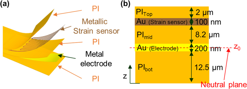
Configuration of the stretchable interconnector. : (a) Illustration of exploded stretchable interconnector. (b) Schematics of layer configuration of the stretchable interconnector. The electrode is located on a neutral plane, but the strain sensor is not.
We designed an elastomerically structured substrate for integration into a stretchable circuit. As shown in Fig. 3 (a), the substrate consisted of island and base parts, both cast from the same elastomer composite (25% by weight 17:1 polydimethylsiloxane (PDMS, Sylgard 184, Dow Corning, USA) and 75% by weight Silbione RT Gel 4642 A/B (Silbione, Bluestar Silicone, USA), with Young’s modulus of approximately 80 kPa) but with different thicknesses. This design induces strain concentration in the base parts due to force equilibrium during stretching, as described by the following equation for the strain (ε) in each part.
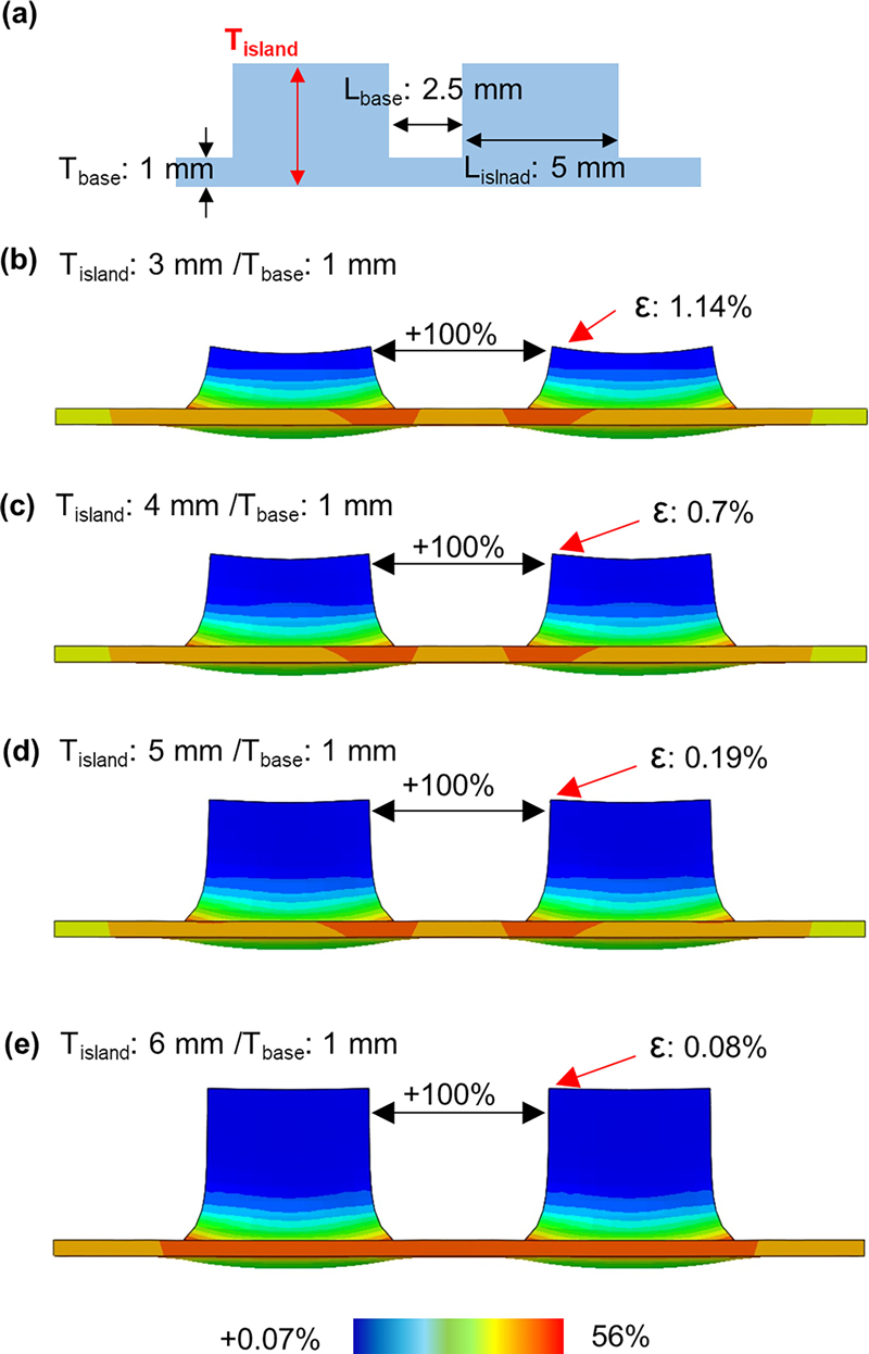
Comparison of the thicknesses of the elastomeric substrate : (a) Schematics of the dimension of the elastomeric substrate (b–e) Finite element method (FEM) result of the elastomeric substrate when stretched to 100% between islands in different thicknesses. (b) Thickness of the island (Tisland): 3 mm, (c) Tisland: 4 mm, (d) Tisland: 5 mm, (e) Tisland: 6 mm
| (1) |
Fig. 3 (b–e) shows the Finite Element Method (FEM) results for the elastomeric substrate when stretched to 100% between islands with varying thicknesses of the island parts. To integrate the stretchable interconnectors, the length of the island parts (Lisland) was set to 5 mm. In addition, to allow the interconnector to stretch by up to 100%, the length of the base (Lbase) was set to 2.5 mm. The thickness of the base (Tbase) was fixed at 1 mm to facilitate demolding. As the thickness of the island parts increases, the maximum strain on the top surface of the islands, where the elastic circuit is integrated, decreases (Tisland: 3 mm → 1.14%, Tisland: 4 mm → 0.7%, Tisland: 5 mm → 0.19%, Tisland: 6 mm → 0.08%). Therefore, to minimize the strain applied to the nondeformable circuit within the stretchable circuit, we selected a thickness of 6 mm for the island parts in the substrate. This resulted in a maximum strain of less than 0.1% on the top surfaces when stretched to 100% between the islands.
Fig. 4 (a) shows the dimensions of the final structured elastomeric substrate. Fig. 4 (b–c) display the FEM results for biaxial stretching at approximately 43% of the structured substrate. The island parts exhibited a minimal strain distribution (<0.1%) compared with the base parts (>50%), which absorbed most of the strain. This substrate structure can withstand tensile deformation while ensuring that the nondeformable circuit is minimally affected by deformation.
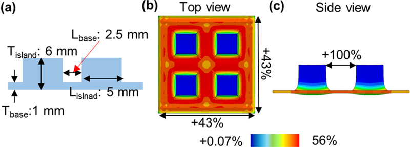
Construction and characteristics of the elastomeric structured substrate. : (a) Schematics of the construction of the elastomeric structured substrate. (b) Top view of the finite element method (FEM) result of the biaxial stretched elastomeric structured substrate. (c) Side view of the FEM result of the biaxial stretched elastomeric structured substrate.
To fabricate stretchable electronics, the structured substrate was prestretched to match the dimensions of the thin-film-based stretchable circuit, as shown in Fig. 5 (a). The structured substrate was designed to have the same dimensions as the stretchable circuit when the base was stretched 100%. After transferring the stretchable circuit onto the prestretched structured substrate (Fig. 5 (b)), pressure was applied to the stretchable circuit using flat glass slides to induce downward bending of the interconnector at the start of the release process. Once slight bending of the interconnector was confirmed, the substrate was gently released, allowing the stretchable interconnectors between the islands to bend fully, as shown in Fig. 5 (c). Although we induced bending of the interconnectors through additional pressing, further research is needed to improve the stability and simplify the process by developing a design that can intrinsically bend downward. The bent stretchable interconnectors can stretch by up to 100%. The stretchability of electronics can be adjusted by modifying the dimensions of the substrate and the stretchable circuit.

Schematics of a fabrication process of the stretchable electronics. : (a) Prepare a thin film-based stretchable circuit onto a prestretched elastomeric structured substrate in alignment. (b) Transfer printing the stretchable circuit onto the substrate. (c) Release the substrate. The stretchable interconnectors are bent along the gap between the structures of the substrate decreases.
3.3 Mechanical and electrical characteristics of the stretchable interconnector.
Stretchable interconnectors bend in the released (normal) state of stretchable electronics. Fig. 6 shows the FEM results for a stretchable interconnector in its bent state. The maximum and minimum strains in the polyimide (PI), excluding the metallic parts, are +2.0% and -2.91%, respectively. These strains are within the 3% yield strain of PI [25]. The maximum and minimum strains applied to the metal electrode inside the stretchable interconnector are +0.17% and -0.26%, respectively, as shown in Fig. 6 (b). Because the metal electrode was positioned at the neutral plane within the stretchable interconnector, the applied strain was minimal, ensuring stable electrical connections for stretchable electronics. By contrast, the strain sensor experienced higher strains than the metal electrode, with maximum and minimum strains of +2.98% and -0.62%, respectively, as shown in Fig. 6 (c). These strains are higher than the yield strain of gold (~1%) but lower than the failure strain (~4%) [26]. This indicates that although small cracks may form in the strain sensor, connectivity is maintained, allowing it to function as a strain sensor against the stretching deformation of the stretchable interconnector.

FEM results of the bent stretchable interconnector. : (a) FEM result of the bent (released) stretchable interconnector. The strain sensors are located at both ends of the interconnector. Radius of the interconnector (R) : ~0.5 mm (b) FEM result of the electrode in stretchable interconnector. (c) FEM result of the strain sensor in stretchable interconnector. Color bars indicates the strain distribution of the model.
We positioned the two strain sensors near both ends of the interconnector to be affected by convex bending. If the strain sensor is placed along the entire length of the interconnector, it is affected by both convex and concave bending, thereby reducing the range of resistance changes. When the strain sensor is located at the center of the interconnector, the bending stiffness of the strain sensor results in a radius of ~0.92 mm in the released interconnector, which is larger than the radius when the sensors are placed at both ends (R: ~0.5 mm), as shown by the FEM results in Fig. 7 (a). The maximum and minimum strains of the center-located strain sensor were +0.22% and -2.33%, respectively, as shown in Fig. 7 (b). Although both the center- and end-located strain sensors exhibited similar absolute maximum strain values, the end-located strain sensor arrangement allowed for the integration of two sensors at both ends of the interconnector, thereby enhancing the sensitivity.
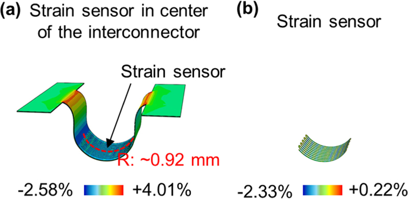
FEM results of the bent stretchable interconnector with the strain sensor positioned at the center of the interconnector. (a) FEM result of the bent (released) stretchable interconnector with strain sensor positioned at center of the interconnector. Radius of the interconnector (R): ~0.92 mm. (b) FEM result of the strain sensor positioned at the center of the interconnector. Color bars indicates the strain distribution of the model.
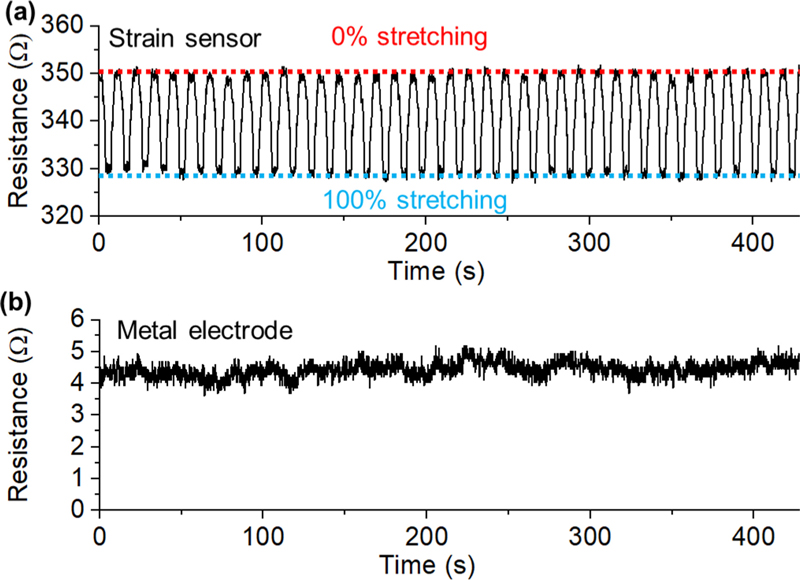
Fig. 8 (a) and 8 (b) show optical images of the stretchable electronics before and after 100% stretching of the interconnector. The stretchable interconnector transitioned from a bent to a flat structure during stretching. As shown in Fig. 8 (c), the resistance of the strain sensor before stretching was approximately 350 Ω (red box), gradually decreasing to approximately 330 Ω (yellow box) as the interconnector stretched. At 100% stretching, the resistance of the strain sensor stabilized at approximately 330 Ω (blue box). Upon returning from 100% to 0% stretching, the resistance gradually increased back to ~350 Ω, the same value as before stretching. By contrast, the metal electrode showed no observable resistance changes during the same stretching deformations, maintaining a stable resistance of approximately 4.3 Ω, as shown in Fig. 8 (d).
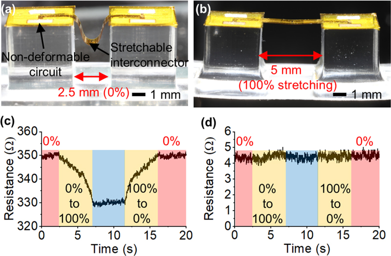
Electromechanical characteristics of the stretchable interconnector. : (a) Optical image of the stretchable interconnector. (b) Optical image of the stretchable interconnector when 100% stretching. (c, d) Resistance change of (c) the strain sensor and (d) the electrode in the stretchable interconnector along the stretching deformations.
When the stretchable interconnector was stretched incrementally by 20% from 0% to 100%, the resistance of the strain sensor did not change at regular intervals, but instead exhibited distinguishable gradual variations, as shown in Fig. 9 (a). The gauge factor (GF) was calculated to be approximately -0.06. The metal electrode exhibited no significant resistance changes under any of the stretching conditions, as shown in Fig. 9 (b).
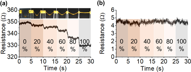
Resistance changes of the stretchable interconnector along the stretching deformation. : (a) Resistance change of the strain sensor along the step-by-step stretching deformations and corresponding optical images. (b) Resistance change of the electrode along the step-by-step stretching deformations.
Under repetitive deformation conditions, during 50 cycles of 100% stretching of the stretchable interconnector followed by a release to 0%, the resistance of the strain sensor displayed consistent changes, as shown in Fig. 10 (a). Simultaneously, the resistance of the metal electrode remained stable throughout the 50 stretching cycles (Fig. 10 (b)).
3.4 Demonstration of the self-sensible stretchable 3 × 3 LED matrix as an application of the stretchable electronics with strain sensor.
The designed stretchable electronics with a strain sensor feature stretchable interconnectors that absorb the entire strain during deformation. The resistance of the resistive strain sensor embedded in the stretchable interconnector changes in response to stretching deformation, enabling a self-sensing function.
To demonstrate this self-sensing capability, we designed a stretchable 3 × 3 passive LED matrix circuit as shown in Fig. 11 (a). The LEDs were positioned on the nondeformable circuits located on the island parts of the elastomerically structured substrate, with the stretchable interconnectors providing electrical connections between the nondeformable circuits to form the passive LED matrix. Each stretchable interconnector included a resistive strain sensor to detect the stretching deformation of the interconnector.
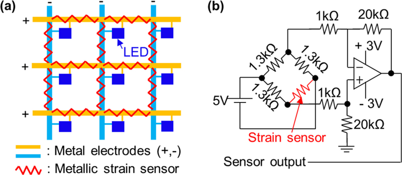
(a) Schematics of the stretchable 3 × 3 light-emitting diode (LED) matrix with strain sensors. (b) Circuit diagram for converting resistance changes of strain sensor to amplified voltage changes.
To measure and convert the resistance changes of the strain sensor into an analog input for the microcontroller unit (MCU, Arduino Mega, Arduino, USA), we incorporated a Wheatstone bridge circuit with a noninverting amplifier, as illustrated in Fig. 11 (b).
We designed an operational procedure to sequentially turn on the LEDs in the direction of matrix stretching. As shown in Fig. 12 (a–f), when the LED matrix was stretched laterally (x-axis), the resistance of the strain sensor decreased in that direction. The LEDs in the first row were sequentially turned on based on the strain sensor output values corresponding to different levels of stretching (≥0%, ≥15%, ≥30%), as shown in Fig. 12 (a–c). After 30% lateral stretching, the LED matrix was stretched vertically (y-axis). As the resistance of the strain sensor in the vertical direction decreases, the LEDs in the second and third rows are sequentially activated, as shown in Fig. 12 (d–f).
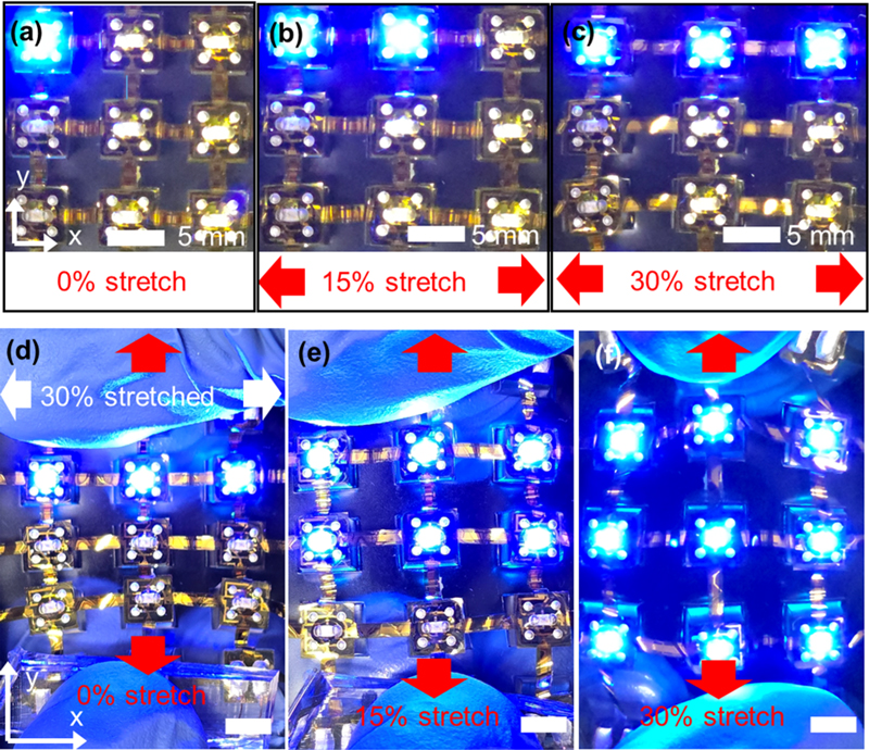
Demonstration of the stretchable 3 × 3 LED matrix with strain sensors. : (a–c) Optical images of sequential LED lighting against lateral stretching of the LED matrix. (a) 0%, (b) 15%, (c) 30% lateral stretching. (d–f) Optical images of sequential LED light against vertical stretching of the LED matrix after 30% lateral stretching. (d) 0%, (e) 15%, (f) 30% vertical stretching. Scale bar: 5 mm.
Fig. 13 shows the wrapping of a rod (radius: 7 mm) with a stretchable 3 × 3 LED matrix using an integrated strain sensor. The LEDs were designed to operate sequentially from the left to the right column in response to the stretching ratio of the matrix. When the matrix is flat, only the LEDs in the left column are turned on, as shown in Fig. 13 (a). As the rod was gradually wrapped, the LEDs in the second and third columns were sequentially activated because of the stretching of the interconnectors, as shown in Fig. 13 (b) and 13 (c).
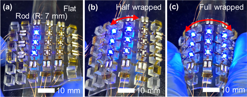
Rod wrapping with the stretchable 3 × 3 LED matrix with strain sensors. : (a) Flat state of the LED matrix on the rod. (b) Rod half wrapped with the LED matrix. (c) Rod full wrapped with the LED matrix. The LEDs were sequentially turned on along the stretching of the strain sensor in the stretchable interconnector.
4. CONCLUSIONS
Herein, we presented a strategy for embedding strain sensors in stretchable electronics, enabling the self-sensing of stretchability. Through a sophisticated design that considers the neutral plane of the stretchable interconnector, both a stable electrode and a resistive strain sensor that endures stretching deformations can be incorporated. Both computational and experimental analyses verified the stable operation of the electrode and strain sensor embedded in the same stretchable interconnector. The stretchable 3 × 3 LED matrix with the strain sensor demonstrated the feasibility of the self-sensing function of stretchable electronics.
Although we have successfully demonstrated notable stretchable electronics, some challenges remain unaddressed. First, the gauge factor of metal-based strain sensors is lower than that of commonly used strain sensors. Improving the design of the strain sensors or using intrinsically stretchable materials such as carbon nanotubes [27] or silver nanowires [28] may result in more sophisticated sensing properties with a higher gauge factor. Second, the mechanically guided fabrication procedure for stretchable electronics must be improved to enhance reproducibility and ensure stable functionality. Geometrical and experimental analyses of the designs of stretchable interconnectors and islands may enhance stretchability and predict the structure of the interconnectors at the start of the release process, thereby improving sensitivity and stability [29]. Third, for practical applications, electronics require thin structures to prevent mechanical failures during daily use. To address this, we may consider an elastomeric substrate with a bonded structure composed of two or more elastomers of different moduli [30]. A higher-modulus elastomer would be less affected by deformation than a lower-modulus elastomer, achieving a similar effect on thickness control in our study. This could be a valuable method for reducing the thickness.
Nonetheless, integrating additional functions into the stretchable interconnectors of rigid conductor-based stretchable electronics can enhance their functional density, which often decreases their stretchability. Additionally, the self-sensing design of stretchable electronics has significant potential for applications in proprioceptive electronics. Further development of our approach to embedding functions in stretchable interconnectors should lead to more feasible applications with advanced functionalities in stretchable electronics.
Acknowledgments
This work was supported by the Korea Evaluation Institute of Industrial Technology (KEIT) grant funded by the Korean government (MOTIE, Grant No. RS-2022-00154781, Development of large-area wafer-level flexible/stretchable hybrid sensor platform technology for form-factor-free highly integrated convergence sensor).
References
-
J. A. Rogers, T. Someya, and Y. Huang, “Materials and mechanics for stretchable electronics”, Sci., Vol. 327, No. 5973, pp. 1603-1607, 2010.
[https://doi.org/10.1126/science.1182383]

-
D. H. Kim and J. A. Rogers, “Stretchable electronics: materials strategies and devices”, Adv. Mater., Vol. 20, No. 24, pp. 4887-4892, 2008.
[https://doi.org/10.1002/adma.200801788]

-
N. Lu and S. Yang, “Mechanics for stretchable sensors”, Curr. Opin. Solid State Mater. Sci., Vol. 19, No. 3, pp. 149-159, 2015.
[https://doi.org/10.1016/j.cossms.2014.12.007]

-
J. Byun, Y. Lee, J. Yoon, B. Lee, E. Oh, S. Chung, T. Lee, K. J. Cho, J. Kim, and Y. Hong, “Electronic skins for soft, compact, reversible assembly of wirelessly activated fully soft robots”, Sci. Robot., Vol. 3, No. 18, p. eaas9020, 2018.
[https://doi.org/10.1126/scirobotics.aas9020]

-
J. H. Koo, D. C. Kim, H. J. Shim, T. H. Kim, and D. H. Kim, “Flexible and Stretchable Smart Display: Materials, Fabrication, Device Design, and System Integration”, Adv. Funct. Mater., Vol. 28, No. 35, p. 1801834, 2018.
[https://doi.org/10.1002/adfm.201801834]

-
J. Lee, B. L. Zambrano, J. Woo, K. Yoon, and T. Lee, “Recent Advances in 1D Stretchable Electrodes and Devices for Textile and Wearable Electronics: Materials, Fabrications, and Applications”, Adv. Mater., Vol. 32, No. 5, p. 1902532, 2020.
[https://doi.org/10.1002/adma.201902532]

-
B. L. Zambrano, A. F. Renz, T. Ruff, S. Lienemann, K. Tybrandt, J. Voros, and J. Lee. “Soft Electronics Based on Stretchable and Conductive Nanocomposites for Biomedical Applications”, Adv. Healthc. Mater., Vol. 10, No. 3, p. 2001397, 2021.
[https://doi.org/10.1002/adhm.202001397]

-
W. Hong, C. Jiang, M. Qin, Z. Song, P. Ji, L. Wang, K. Tu, L. Lu, Z. Guo, B. Yang, X. Wang, and J. Liu, “Self-adaptive cardiac optogenetics device based on negative stretching-resistive strain sensor”, Sci. Adv., Vol. 7, No. 48, p. eabj4273, 2021.
[https://doi.org/10.1126/sciadv.abj4273]

-
Z. Huang, Y. Hao, Y. Li, H. Hu, C. Wang, A. Nomoto, T. Pan, Y. Gu, Y. Chen, T. Zhang, W. Li, Y. Lei, N. H. Kim, C. Wang, L. Zhang, J. W. Ward, A. Maralani, X. Li, M. F. Durstock, A. Pisano, Y. Lin, and S. Xu, “Three-dimensional integrated stretchable electronics”, Nat. Electron., Vol. 1, No. 8, pp. 473-480, 2018.
[https://doi.org/10.1038/s41928-018-0116-y]

-
D. G. Marques, P. A. Lopes, A. T. de Almeida, C. Majidi, and M. Tavakoli, “Reliable interfaces for EGaIn multi-layer stretchable circuits and microelectronics”, Lab. Chip, Vol. 19, No. 5, pp. 897-906, 2019.
[https://doi.org/10.1039/C8LC01093E]

-
A. Larmagnac, S. Eggenberger, H. Janossy, and J. Voros, “Stretchable electronics based on Ag-PDMS composites”, Sci. Rep., Vol. 4, No. 1, p. 7254, 2014.
[https://doi.org/10.1038/srep07254]

-
J. Lv, G. Thangavel, and P. S. Lee, “Reliability of printed stretchable electronics based on nano/micro materials for practical applications”, Nanoscale, Vol. 15, No. 2, pp. 434-449, 2023.
[https://doi.org/10.1039/D2NR04464A]

-
H. Song, G. Luo, Z. Ji, R. Bo, Z. Xue, D. Yan, F. Zhang, K. Bai, J. Liu, X. Cheng, W. Pang, Z. Shen, and Y. Zhang, “Highly-integrated, miniaturized, stretchable electronic systems based on stacked multilayer network materials”, Sci. Adv., Vol. 8, No. 11, p. eabm3785, 2022.
[https://doi.org/10.1126/sciadv.abm3785]

-
G. Lee, M. Zarei, Q. Wei, Y. Zhu, and S. G. Lee, “Surface Wrinkling for Flexible and Stretchable Sensors”, Small, Vol. 18, No. 42, p. 2203491, 2022.
[https://doi.org/10.1002/smll.202203491]

-
Y. Li, W. Liu, Y. Deng, W. Hong, and H. Yu, “Miura-ori enabled stretchable circuit boards”, Npj Flex. Electron., Vol. 5, No. 3, pp. 1-9, 2021.
[https://doi.org/10.1038/s41528-021-00099-8]

-
J. P. Rojas, M. U. Rehman, A. Hussein, A. E’mar, Y. AlRaei, H. AlZaher, and M. Mohandes, “Kirigami-Enabled Wearable Health and Crowd Monitoring System”, Arab. J. Sci. Eng., Vol. 47, No. 3, pp. 3583-3595, 2022.
[https://doi.org/10.1007/s13369-021-06384-y]

-
B. C. K. Tee and J. Ouyang, “Soft Electronically Functional Polymeric Composite Materials for a Flexible and Stretchable Digital Future”, Adv. Mater., Vol. 30, No. 47, p. 1802560, 2018.
[https://doi.org/10.1002/adma.201802560]

-
G. Li, M. Zhang, S. Liu, M. Yuan, J. Wu, M. Yu, L. Teng, Z. Xu, J. Guo, G. Li, Z. Liu, and X. Ma, “Three-dimensional flexible electronics using solidified liquid metal with regulated plasticity”, Nat. Electron., Vol. 6, No. 2, pp. 154-163, 2023.
[https://doi.org/10.1038/s41928-022-00914-8]

-
M. Jo, S. Bae, I. Oh, J. Jeong, B. Kang, S. J. Hwang, S. S. Lee, H. J. Son, B. M. Moon, M. J. Ko, and P. Lee, “3D Printer-Based Encapsulated Origami Electronics for Extreme System Stretchability and High Areal Coverage”, ACS Nano, Vol. 13, No. 11, pp. 12500-12510, 2019.
[https://doi.org/10.1021/acsnano.9b02362]

-
Y. Su, Z. Liu, S. Kim, J. Wu, Y. Huang, and J. A. Rogers, “Mechanics of stretchable electronics with high fill factors”, Int. J. Solid. Struct., Vol. 49, No. 23-24, pp. 3416-3421, 2012.
[https://doi.org/10.1016/j.ijsolstr.2012.07.024]

-
Y. Liu, Y. Zhong, and C. Wang, “Recent advances in self-actuation and self-sensing materials: State of the art and future perspectives”, Talanta, Vol. 212, p. 120808, 2020.
[https://doi.org/10.1016/j.talanta.2020.120808]

-
D. Li, J. Zhou, K. Yao, S. Liu, J. He, J. Su, Q. Qu, Y. Gao, Z. Song, C. Yiu, C. Sha, Z. Sun, B. Zhang, J. Li, L. Huang, C. Xu, T. H. Wong, X. Huang, J. Li, R. Ye, L. Wei, Z. Zhang, X. Guo, Y. Dai, Z. Xie, and X. Yu, “Touch IoT enabled by wireless self-sensing and haptic-reproducing electronic skin”, Sci. Adv., Vol. 8, No. 51, p. eade2450, 2022.
[https://doi.org/10.1126/sciadv.ade2450]

-
M. Kashif, S. Murshid, and B. Singh, “Solar PV Array Fed Self-Sensing Control of PMSM Drive with Robust Adaptive Hybrid SOGI Based Flux Observer for Water Pumping”, IEEE Trans. Ind. Electron., Vol. 68, No. 8, pp. 6962-6972, 2020.
[https://doi.org/10.1109/TIE.2020.3003656]

-
L. Qin, Y. Tang, U. Gupta, and J. Zhu, “A soft robot capable of 2D mobility and self-sensing for obstacle detection and avoidance”, Smart Mater. Struct., Vol. 27, No. 4, p. 045017, 2018.
[https://doi.org/10.1088/1361-665X/aab393]

-
C. T. Kuo, M. C. Yip, K. N. Chiang, and C. Tsou, “Characterization study of time-and temperature-dependent mechanical behavior of polyimide materials in electronic packaging applications”, J. Electron. Mater., Vol. 34, No. 1, pp. 272-281, 2005.
[https://doi.org/10.1007/s11664-005-0213-3]

-
X. M. Luo and G. P. Zhang, “Deformation-mechanism dependent stretchability of nanocrystalline gold films on flexible substrates”, J. Mater. Res., Vol. 32, No. 18, pp. 3516-3523, 2017.
[https://doi.org/10.1557/jmr.2017.349]

-
T. Yamada, Y. Hayamizu, Y. Yamamoto, Y. Yomogida, A. Izadi-Najafabadi, D. N. Futaba, and K. Hata, “A stretchable carbon nanotube strain sensor for human-motion detection”, Nat. Nanotechnol., Vol. 6, No. 5, pp. 296-301, 2011.
[https://doi.org/10.1038/nnano.2011.36]

-
M. Amjadi, A. Pichipajongkit, S. Lee, S. Ryu, and I. Park, “Highly stretchable and sensitive strain sensor based on silver nanowire–elastomer nanocomposite”, ACS Nano, Vol. 8, No. 5, pp. 5154-5163, 2014.
[https://doi.org/10.1021/nn501204t]

-
J. Ahn, J. H. Ha, Y. Jeong, Y. Jung, J. Choi, J. Gu, S. H. Hwang, M. Kang, J. Ko, S. Cho, H. Han, K. Kang, J. Park, S. Jeon, J. H. Jeong, and I. Park, “Nanoscale three-dimensional fabrication based on mechanically guided assembly”, Nat. Commun., Vol. 14, No. 1, p. 833, 2023.
[https://doi.org/10.1038/s41467-023-36302-9]

-
R. Moser, G. Kettlgruber, C. M. Siket, M. Drack, I. M. Graz, U. Cakmak, Z. Major, M. Kaltenbrunner, and S. Bauer, “From Playroom to Lab: Tough Stretchable Electronics Analyzed with a Tabletop Tensile Tester Made from Toy-Bricks”, Adv. Sci., Vol. 3, No. 4, p. 1500396, 2016.
[https://doi.org/10.1002/advs.201500396]

