Effect of SAW-IDT Electrodes Composed of Aluminum-Nickel Composite Thin Films on the Acoustic Performance of SAW Devices
This is an Open Access article distributed under the terms of the Creative Commons Attribution Non-Commercial License(https://creativecommons.org/licenses/by-nc/3.0/) which permits unrestricted non-commercial use, distribution, and reproduction in any medium, provided the original work is properly cited.
Abstract
Al-Ni thin films were fabricated using combinatorial sputtering system to realize highly sensitive surface acoustic wave (SAW) devices. The Al-Ni sample library was grown with various chemical compositions and electrical resistivities, which provided important information for selecting the most suitable materials for SAW devices. As acoustic waves generated from piezoelectric materials are significantly affected by the resistivity and density of the interdigital transducer (IDT) electrodes, three types of Al-Ni thin films with different Al contents were fabricated. The thickness of the Al-Ni thin film used in the SAW-IDT electrode was fixed at 100 nm. As the Al content of the Al-Ni film decreased from 79.2 to 24.5 at%, the resistivity increased slightly from 4.8 to 5.8 × 10⁻⁵ Ω-cm, whereas the calculated density increased significantly from 3.6 to 6.9 g/cm3. The SAW device composed of Al-Ni IDT electrodes resonated at 71 MHz without frequency shifts; however, the selectivity of the resonant frequency and insertion loss deteriorated as the Al content decreased. When there is no significant difference in the electrical characteristics of the SAW-IDT electrodes, the performance of the SAW devices can be determined by the density of the IDT electrodes.
Keywords:
Surface acoustic wave, Interdigital transducer, Combinatorial RF magnetron sputtering, Aluminum-nickel composite thin film1. INTRODUCTION
Surface acoustic waves (SAWs) are elastic waves that travel along the surface of a piezoelectric material, and were first discovered by Rayleigh in 1885 [1]. In 1965, White and Voltmer’s study into the development of SAWs utilizing a piezoelectric substrate was a technological advance that provided a new direction to tools based on SAWs [2]. An interdigital transducer (IDT), one of the core components of a SAW device, consists of two interlocking comb-shaped metal electrodes deposited on a piezoelectric material. When a sinusoidal wave is applied to the SAW device, the piezoelectric material beneath the IDT vibrates owing to the inverse piezoelectric effect, and at this time, the electrical energy is converted into acoustic energy, generating an acoustic wave perpendicular to the IDT [3,4]. SAW devices have been used in various products, including as filters in wireless radio transmission, spectrum duplexers, radio frequency (RF) identification tags, biological sensors, medical research, as microsensors for the measurement of physical parameters and biochemical detection in biomedical, engineering, and biological sciences [5,6], as microactuators for microfluidic devices [7,8], and lab-on-a-chip applications [9].
Microfluidic devices have attracted considerable attention in the field of biosensing. Owing to their ability to precisely control very small amounts of samples and reagents, such as during separation and mixing, these devices are excellent platforms for performing detection with high resolution and sensitivity [10]. Recently, various technologies, such as electrowetting, magnetics, and optics, have been widely integrated into microfluidics to precisely manipulate fluids inside microchannels, leading to significant progress in the SAW technology [11].
In terms of the electrode structure, SAW-based sensors typically consist of a pair of IDTs with opposite directions, one as the input IDT and the other as the output. The SAW velocity change between the input and output IDTs is characterized by a phase shift and amplitude difference, and is expressed as an oscillating electrical signal of the output based on the inverse piezoelectric effect [12]. SAW sensors are composed of a single metal, such as gold or aluminum, on a LiNbO3 piezoelectric substrate. Au-IDT electrodes with a density of 19.3 g/cm3 have excellent electrical properties, but suppress the generation of vibration frequencies in SAW devices. On the other hand, Al-IDT electrodes have a low density, making it relatively easy to generate acoustic waves; however, their poor electrical properties increase the resistance of SAW devices. Therefore, to overcome the shortcomings of single IDT electrodes, the development of composite materials that simultaneously satisfy the electrical and mechanical properties is necessary to improve the performance of SAW devices.
Typically, SAW-IDT electrodes are fabricated using two processes: electron-beam (e-beam) evaporation and DC/RF sputtering. Although e-beam evaporation is optimized for growing various types of single-metal thin films, problems, such as phase changes, may occur during the growth of multicomponent thin films owing to the difference in melting points between the materials. The DC/RF sputtering method can be used to grow thin films without temperature limitations using various metallic or nonmetallic materials, making it suitable for the implementation of composite thin films with various physical properties. In particular, combinatorial sputtering can produce thin films with compositional gradients in a one-pot process, making it useful for exploring optimized materials [13,14].
This study focused on whether the performance of SAW devices can be improved by replacing conventional single-metal IDT electrodes with composite metal films. Compositionally graded Al-Ni composite films deposited from Al and Ni metal targets were fabricated using combinatorial RF magnetron sputtering. Changes in the chemical, electrical, and mechanical properties of the Al-Ni sample library were closely investigated, and their relationships with the acoustic properties, such as resonant frequency and insertion loss, were systematically elucidated.
2. EXPERIMENTAL
Al-Ni thin films with different chemical, structural, and electrical properties were grown on 4-inch silicon substrates via combinatorial RF sputtering (ULVAC MB07-4501), and their application as SAW-IDT electrodes was systematically investigated. To obtain the Al-Ni thin films, single-metal Al and Ni targets were used, and the Al-Ni thin films were grown in a fixed state without rotating the substrate to obtain a compositional gradient. The sputtering conditions for the compositionally graded Al–Ni thin films were as follows: RF powers of 100 W (Al) and 200 W (Ni), a base pressure of 3.1 × 10⁻⁶ Pa, a working pressure of 0.21 Pa, a flow gas of Ar (99.99%), and a substrate temperature of room temperature. The Al-Ni thin films were cut into five pieces, and the structural, chemical, and electrical properties of each sample were evaluated. In addition, three types of Al-Ni thin films with a uniform Al content were deposited on a 4-inch Si substrate through rotational growth. The growth conditions for the Al-Ni thin films with a uniform Al content were as follows: RF powers of 100 W (Al) and 100, 200, 300 W (Ni), a base pressure of 3 × 10⁻⁶ Pa, a working pressure of 0.21 Pa, a flow gas of Ar (99.99%), and a substrate temperature of room temperature. The SAW-IDT pattern with a straight type was designed to have a resonant frequency of 71 MHz, which consists of an Al-Ni film thickness of 100 nm, a pattern width of 14 μm, a total IDT length of 3000 μm, and 87 electrode pairs. The IDT electrode was patterned on a 4-inch dia. The LiNbO3 substrate, which had a crystal orientation of 128°, rotated from the +Y direction through the +Z axis about the X-axis. Before the deposition of the IDT electrodes, the LiNbO3 wafer was cleaned using a piranha solution, and then, IDT patterns were formed via photolithography with a positive photoresist (AZ GXR 601). The IDT patterns of the Al-Ni thin films were deposited via RF magnetron sputtering. The compositional distribution and morphological properties of the Al-Ni thin films were examined using field-emission scanning electron microscopy (Quanta 200). The electrical resistivity was determined by a Hall effect measurement system using the van der Pauw geometry (Model 7707, Lake Shore Cryotronics) at a constant magnetic field of 4 kG. The IDT patterns were observed using a 3D laser optical microscope (Model OLS4100-SAA, OLYMPUS). The resonant frequency of the SAW device was analyzed using a vector network analyzer (Model E5080B, Keysight).
3. RESULTS AND DISCUSSIONS
Al-Ni thin films with compositional gradients were fabricated using combinatorial RF magnetron sputtering. Fig. 1 shows a schematic of the combinatorial sputtering system used to obtain the Al-Ni thin films with compositional gradients. Note that Al-Ni thin films can be grown with alternating compositions while maintaining a constant thickness, depending on the sample position. The Al-Ni sample library can minimize errors that may occur owing to the film thickness and observe only the changes in the material properties according to the composition at the same film thickness. The surface and cross-sectional morphologies of the Al-Ni thin films with different compositions and constant film thicknesses are shown in Fig. 2.
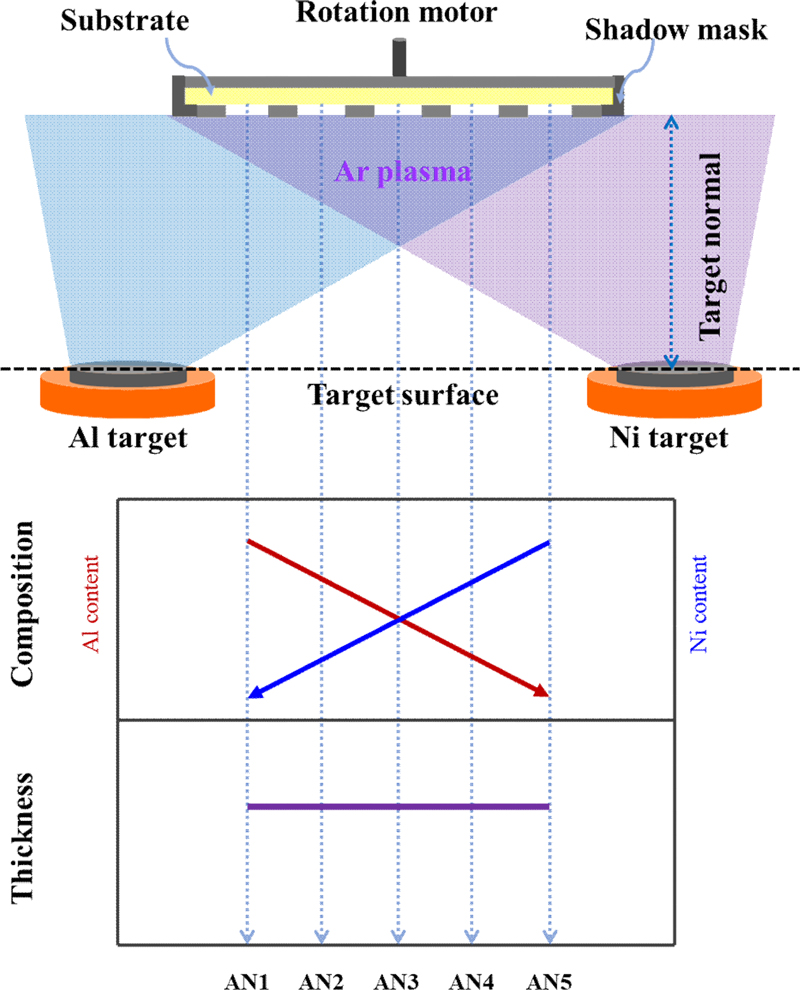
Schematic of the combinatorial sputtering system to obtain the Al-Ni thin films with compositional gradients.
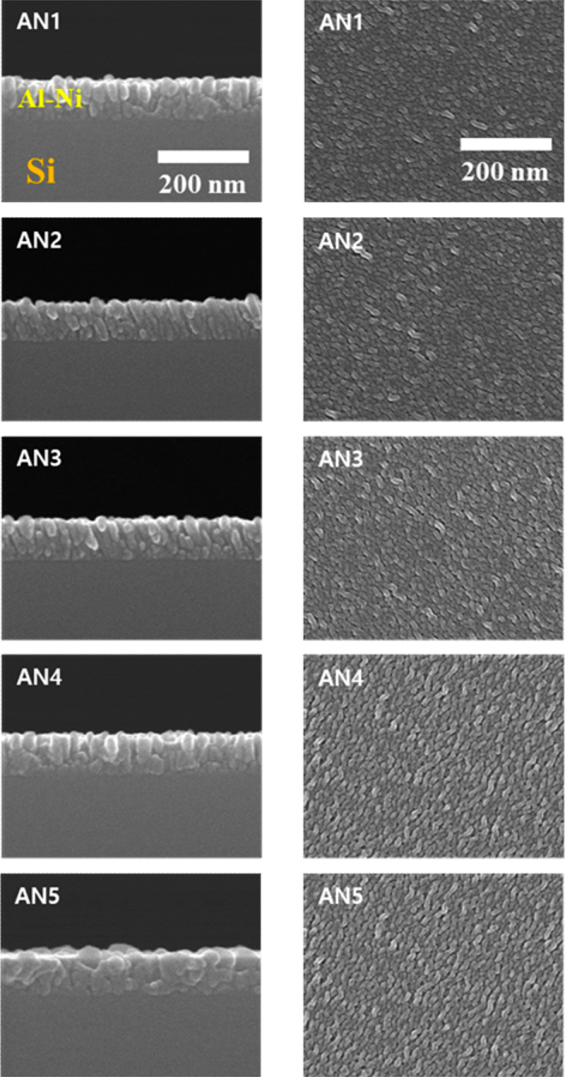
Surface and cross-sectional morphologies of the Al-Ni thin films as a function of the sample position.
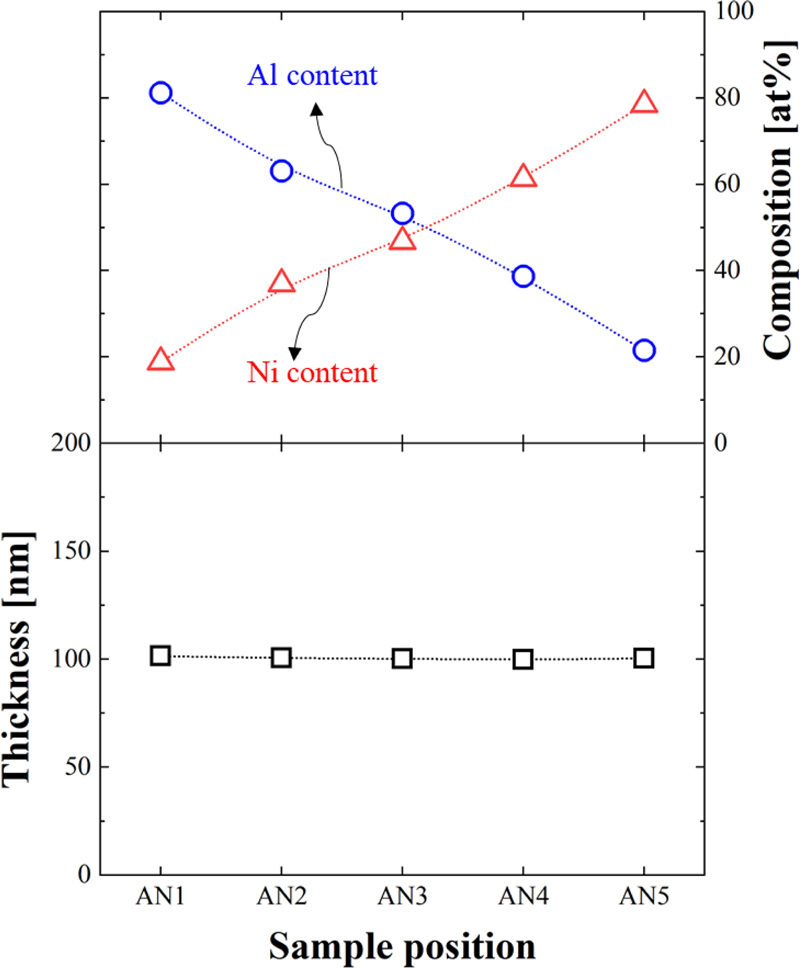
The AN1 thin film was located near the Al target, whereas the AN5 thin film was located near the Ni target. The Al-Ni thin films showed excellent adhesion to the substrate regardless of the sample position, and no defects, such as voids or cracks, were observed at either the surface or the interface. As shown in Fig. 3, all the Al-Ni films were grown to a constant film thickness, indicating that the Al-Ni thin films were distributed with a thickness of approximately 100 nm, regardless of the sample position.
However, the compositions of the Al-Ni films intersect almost linearly with the sample position, and each sample has different Al and Ni contents. As the number of samples increased, the Al content decreased from 81.2% to 25.6% and the Ni content increased from 18.8% to 75.4%.
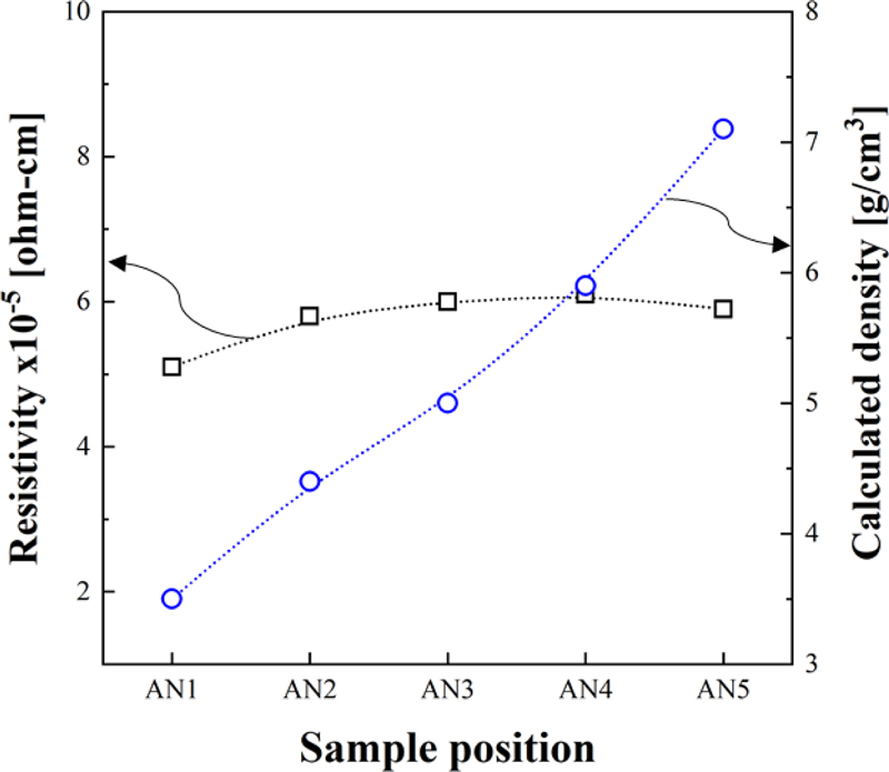
Fig. 4 shows the resistivity and calculated density of the Al-Ni thin films as functions of the sample position. The resistivity of the Al-Ni thin films was distributed from 5.1 to 5.9 × 10⁻⁵ Ω-cm as the sample number increased, without a significant change. On the other hand, the calculated density changed significantly from 3.5 to 7.1 g/cm3 as the sample number increased. The mixed densities of the Al-Ni thin films were calculated using the following equation:
where ρ represents the theoretical density, and V represents the volume percentage. The densities of the Al-Ni mixed thin films were calculated by converting the atomic percentages of the five Al-Ni samples with varying Al and Ni contents to volume percentages. As shown in Fig. 1, the compositions of the Al-Ni thin films with the same thickness were linearly distributed according to the sample position. Based on these results, the effect of the density of the Al-Ni IDT electrodes with the same film thickness and resistivity on the acoustic characteristics of the SAW device was investigated.
Through combinatorial studies, it was confirmed that the electrical and mechanical properties of the Al-Ni thin films vary with the Al content at the same film thickness. To form the SAW-IDT electrode, Al-Ni thin films with uniform composition should be prepared over the entire substrate. Therefore, three different types of compositionally uniform Al-Ni thin films were sputtered via rotational growth.
Fig. 5 shows the cross-sectional morphology, composition, resistivity, and density of the three types of Al-Ni thin films grown on a Si substrate. The three types of Al-Ni thin films had an average film thickness of 102 nm, and no structural defects, such as voids or cracks, were observed between the substrate and the film. Similar to the Al-Ni sample series with compositional gradients, when the composition of the Al-Ni thin films changed abruptly from 79.2 to 24.5 at%, the resistivity increased slightly from 4.8 to 5.8 × 10⁻⁵ Ω-cm, but the calculated density increased significantly from 3.6 to 6.9 g/cm3.
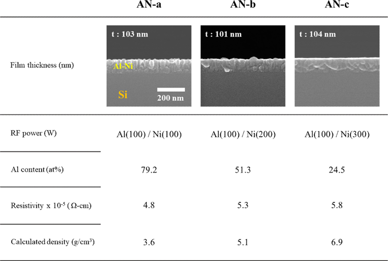
Cross-sectional morphology, composition, resistivity, and calculated density of Al-Ni thin films with various Al contents.
Various analyses of Al-Ni thin films are ultimately aimed at selecting a high-performance SAW-IDT electrode material that can precisely control the particles in microfluidics. Therefore, the polymer material used in SAW-based microfluidics was selected as spherical polystyrene (PS) microparticles with a diameter of 10 μm. To control solid objects in microfluidics, it is necessary to satisfy the Mie scattering condition because the Helmholtz number (k) is determined by the relationship between the diameter of the solid object and the resonant frequency. Hence, the resonant frequency for controlling 10 μm PS particles in microfluidics was calculated using the following equation [15]:
where k is the Helmholtz number, f is the resonant frequency, and cf is the acoustic wave speed in pure water. When the k value satisfying the Mie scattering condition was 1.5, the resonant frequency that can control 10 μm PS particles was confirmed to be 71 MHz. To obtain the resonant frequency suitable for the separation of 10 μm PS particles, the acoustic frequency was calculated using the following equation [16]:
where cs is the speed of acoustic waves in the piezoelectric substrate, and λ is the wavelength of SAWs. The wavelength of the SAWs is dependent on the structure of the IDTs, which can be calculated as [16]
where λ is the wavelength of the SAWs, and d is the width of the IDTs (assuming the width and spatial distance of the IDTs are the same).
Based on the above relationships, the correlation between the IDT pattern width, the number of IDT electrodes, film thickness, and total electrode length was clarified using Mathematica, and the influence on the intensity and frequency of the acoustic waves generated from the SAW device was investigated. The resonant frequency corresponding to the IDT pattern width was analyzed using the above equation, and the SAW-IDT pattern width of 14 um is required to achieve a resonant frequency of 71 MHz. Fig. 6 shows the relationship between the number of IDT electrode pairs and the total IDT length for the impedance matching of the SAW module. In this study, 87 IDT electrode pairs and the total IDT length of 3000 μm were selected to satisfy the reference impedance of 50 Ω.
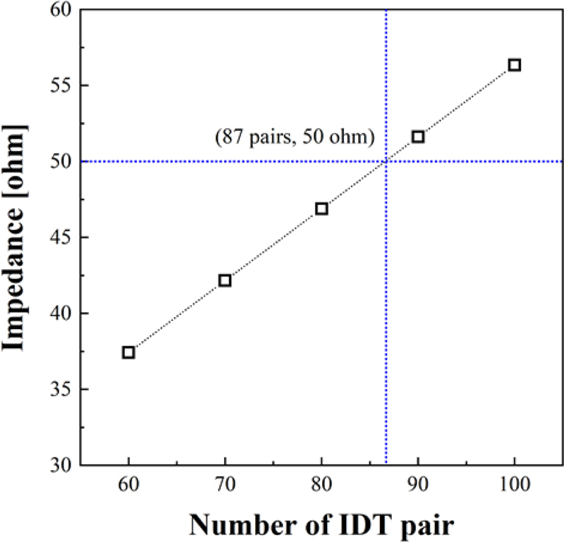
Relationship between the number of IDT electrode pairs and total IDT length for the impedance matching of the SAW module.
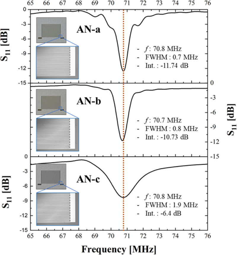
Fig. 7 shows the SAW devices and their resonant frequencies fabricated with the Al-Ni thin films with different Al contents of 79.2 (sample number; AN-a), 51.3 (sample number; AN-b), and 24.5 (sample number; AN-c) at%. All three types of SAW devices have the same pattern width of 14 μm, total IDT length of 3000 μm, film thickness of 100 nm, and 87 electrode pairs. All the three SAW devices exhibited the same resonant frequency of approximately 71 MHz, confirming that they were fabricated normally without defects in the designed IDT patterns. As the Al content of the IDT electrode composed of Al-Ni thin films decreased, the insertion loss at the resonant frequency decreased rapidly from -11.7 to -6.4 dB, and the frequency selectivity gradually increased from 0.7 to 1.9 MHz. As mentioned earlier, the resistivity of the IDT electrodes used in the three types of SAW devices showed a slight fluctuation, but showed a constant value of 5.3 × 10⁻⁵ Ω-cm on average. In other words, the acoustic performance of the SAW device is not determined by the electrical or structural characteristics of the IDT electrode, but is affected by the density of the IDT electrode. In other words, the electrical energy applied from the IDT electrode is converted into mechanical energy, which expands or contracts the crystals of the piezoelectric material via the inverse piezoelectric effect. The high density of the IDT electrode formed in the piezoelectric material could locally restrict the generation of acoustic waves, thereby weakening the insertion loss and selectivity of the resonant frequency.
4. CONCLUSIONS
Al-Ni thin films with a compositional gradient were codeposited using a combinatorial sputtering system to select-candidates for the IDT electrodes used in SAW devices. The Al-Ni sample library exhibited various chemical compositions and electrical resistivities depending on the sample position. Three uniform Al-Ni thin films were grown on Si substrates to verify the acoustic performance of the SAW device according to the Al content. The center frequency was observed at 71 MHz, regardless of the Al content of the SAW-IDT electrode; however, the acoustic performance of the SAW device gradually deteriorated as the Al content of the SAW-IDT electrode decreased. The Al-Ni thin film with the Al content of 79.2 at% exhibited the best performance for the SAW devices, with a resistivity of 4.8 × 10⁻⁵ Ω-cm and a density of 3.6 g/cm³. These results demonstrate that reducing the density of the electrodes deposited on the piezoelectric substrate, rather than optimizing the electrical characteristics of the IDT electrode, is more effective in improving the resonance performance of SAW devices.
Acknowledgments
This study was conducted with the support of the Korea Institute of Industrial Technology and the Korea Industrial Complex Corporation as a “Competitiveness reinforcement project for industrial clusters (1415189052).”
References
-
L. Rayleigh, “On Waves Propagated along the Plane Surface of an Elastic Solid”, Proc. of London Math. Soc., pp. 4-11, 1885.
[https://doi.org/10.1112/plms/s1-17.1.4]

-
R. M. White and F. W. Voltmer, “Direct piezoelectric coupling to surface elastic waves”, Appl. Phys. Lett., Vol. 7, No. 12, pp. 314-316, 1965.
[https://doi.org/10.1063/1.1754276]

-
Z. Jiang, B. Liu, L. Yu, Y. Tong, M. Yan, R. Zhang, W. Han, Y. Hao, L. Shangguan, S. Zhang, and W. Li, “Research progresses in preparation methods and applications of zinc oxide nanoparticles”, J. Alloys Compd., Vol. 956, p. 170316, 2023.
[https://doi.org/10.1016/j.jallcom.2023.170316]

-
R. Augustine, F. Sarry, N. Kalarikkal, S. Thomas, L. Badie, and D. Rouxel, “Surface Acoustic Wave Device with Reduced Insertion Loss by Electrospinning P(VDF–TrFE)/ZnO Nanocomposites”, Nanomicro Lett., Vol. 8, pp. 282-290, 2016.
[https://doi.org/10.1007/s40820-016-0088-2]

-
R. Fachberger and A. Erlacher, “Applications of wireless SAW sensing in the steel industry”, Procedia Eng., Vol. 5, pp. 224-227, 2010.
[https://doi.org/10.1016/j.proeng.2010.09.088]

-
Y. Q. Fu, J. K. Luo, X. Y. Du, A. J. Flewitt, Y. Li, G. H. Markx, A. J. Walton, and W. I. Milne, “Recent developments on ZnO films for acoustic wave based bio-sensing and microfluidic applications: a review”, Sens. Actuator B Chem., Vol. 143, No. 2, pp. 606-619, 2010.
[https://doi.org/10.1016/j.snb.2009.10.010]

-
Y. Q. Fu, L. Garcia-Gancedo, H. F. Pang, S. Porro, Y. W. Gu, J. K. Luo, X. T. Zu, F. Placido, J. I. B. Wilson, A. J. Flewitt, and W. I. Milne, “Microfluidics based on ZnO/nanocrystalline diamond surface acoustic wave devices”, Biomicrofluidics, Vol. 6, No. 2, p. 024105, 2012.
[https://doi.org/10.1063/1.3699974]

-
J. K. Luo, Y. Q. Fu, G. Ashley, and W. I. Milne, “Integrated ZnO Film Based Acoustic Wave Microfluidics and Biosensors”, Adv. Sci. Technol., Vol. 67, pp. 49-58, 2011.
[https://doi.org/10.4028/www.scientific.net/AST.67.49]

-
Z. Guttenberg, H. Müller, H. Habermüller, A. Geisbauer, J. Pipper, J. Felbel, M. Kielpinski, J. Scribaa, and A. Wixforthac, “Planar chip device for PCR and hybridization with surface acoustic wave pump”, Lab Chip, Vol. 5, No. 3, pp. 308-317, 2005.
[https://doi.org/10.1039/B412712A]

-
G. M. Whitesides, “The origins and the future of microfluidics”, Nature, Vol. 442, No. 7101, pp. 368-373, 2006.
[https://doi.org/10.1038/nature05058]

-
P. Teng, D. Tian, H. Fu, and S. Wang, “Recent progress of electrowetting for droplet manipulation: from wetting to superwetting systems”, Mater. Chem. Front., Vol. 4, No. 1, pp. 140-154, 2020.
[https://doi.org/10.1039/C9QM00458K]

-
D. L. Arruda, W. C. Wilson, C. Nguyen, Q. W. Yao, R. J. Caiazzo, I. Talpasanu, D. E. Dow, and B. C. S. Liu, “Microelectrical sensors as emerging platforms for protein biomarker detection in point-of-care diagnostics”, Expert Rev. Mol. Diagn., Vol. 9, No. 7, pp. 749-755, 2009.
[https://doi.org/10.1586/erm.09.47]

-
J. C. Park, J. R. Lee, M. Al-Jassim, and T. W. Kim, “Bandgap engineering of Cu(In1-xGax)Se2 absorber layers fabricated using CuInSe2 and CuGaSe2 targets for one-step sputtering process”, Opt. Mat. Express, Vol. 6, No. 11, pp. 3541-3549, 2016.
[https://doi.org/10.1364/OME.6.003541]

-
P. Nagy, M. Wątroba, Z. Hegedűs, J. Michler, L. Pethö, J. Schwiedrzik, Z. Czigány, and J. Gubicza, “Mapping the microstructure and the mechanical performance of a combinatorial Co–Cr–Cu–Fe–Ni–Zn high-entropy alloy thin film processed by magnetron sputtering technique”, J. Mater. Res. Technol., Vo. 31, pp. 47-61, 2024.
[https://doi.org/10.1016/j.jmrt.2024.06.059]

-
R. C. Chanaud, “Effects of Geometry on The Resonance Frequency of Helmholtz Resonators”, J. Sound Vib., Vol. 178, No. 3, pp. 337-348, 1994.
[https://doi.org/10.1006/jsvi.1994.1490]

- J. D. N. Cheeke, Fundamentals and Applications of Ultrasonic Waves, Boca Raton, CRC press, FL, pp. 1-480, 2002.
