CMOS Binary Image Sensor Using Double-Tail Comparator with High-Speed and Low-Power Consumption
This is an Open Access article distributed under the terms of the Creative Commons Attribution Non-Commercial License(https://creativecommons.org/licenses/by-nc/3.0/) which permits unrestricted non-commercial use, distribution, and reproduction in any medium, provided the original work is properly cited.
Abstract
In this paper, we propose a high-speed, low-power complementary metal-oxide semiconductor (CMOS) binary image sensor featuring a gate/body-tied (GBT) p-channel metal-oxide-semiconductor field-effect transistor (PMOSFET)-type photodetector based on a double-tail comparator. The GBT photodetector forms a structure in which the floating gate (n+ polysilicon) and body of the PMOSFET are tied, and amplifies the photocurrent generated by incident light. The double-tail comparator compares the output signal of a pixel against a reference voltage and returns a binary signal, and it exhibits improved power consumption and processing speed compared with those of a conventional two-stage comparator. The proposed sensor has the advantages of a high signal processing speed and low power consumption. The proposed CMOS binary image sensor was designed and fabricated using a standard 0.18 μm CMOS process.
Keywords:
CMOS image sensor, CMOS binary image sensor, GBT PMOSFET-type photodetector, double-tail comparator1. INTRODUCTION
Image sensors convert incident light into electronic signals. The two main types of image sensors are charge-coupled device (CCD) image sensors and complementary metal–oxide–semiconductor (CMOS) image sensors (CIS). CCD image sensors transmit electron signals with light information to an output amplifier that converts electron charge into voltage. CISs convert the electron signal with light information into voltage in the amplifier of each pixel. CISs are widely used in various applications, such as digital single-lens reflex cameras, closed-circuit television cameras, portable devices, and industrial cameras [1–3].
CISs have some disadvantages, such as dark currents in the photodiode and noise in the readout circuit. The noise issues of CISs have been partially mitigated by the development of processing technology. CISs also have advantages, such as lower cost, higher integrability, and higher speed compared with those of CCD image sensors [4-5].
The p-n junction photodiode is fabricated using standard CMOS processes and is thus used in conventional CISs. The proposed gate/body-tied (GBT) p-channel metal–oxide–semiconductor field-effect transistor (PMOSFET)-type photodetector amplifies the photocurrent generated by incident light and thus exhibits a high sensitivity [6,7].
Conventional CISs convert an image signal into a digital signal through an analog-to-digital converter. The proposed binary image sensor converts an image signal into a binary signal through the proposed double-tail comparator. As the binary output of the CMOS binary image sensor contains less information than that contained in the digital signal of the conventional CIS, the CMOS binary image sensor is advantageous for a high-speed, low-power operation [8,9].
In this paper, we propose a high-speed, low-power CMOS binary image sensor with a GBT PMOSFET-type photodetector and a double-tail comparator [10-13]. The proposed GBT PMOSFET-type photodetector has a high sensitivity. The doubletail comparator is used to improve the power consumption and processing speed of the CMOS binary image sensor. Simulation results have confirmed that the characteristics of the double-tail comparator are improved compared with those of a conventional two-stage comparator [10]. In this study, the proposed CMOS binary image sensor was designed and fabricated using a standard 0.18 μm CMOS process. The characteristics of the fabricated CMOS binary image sensor using the double-tail comparator were evaluated.
2. OPERATING PRINCIPLE
2.1 GBT PMOSFET-type photodetector
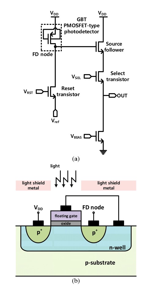
Fig. 1(a) shows the schematic of an active pixel sensor (APS) with a GBT PMOSFET-type photodetector. The APS consists of three n-channel MOSFETs (NMOSFETs) and a GBT PMOSFETtype photodetector. The GBT PMOSFET-type photodetector is configured using the tied floating gate (n+ polysilicon) and n-well body of the PMOSFET. The source follower amplifies the floating diffusion (FD) node voltage, and the reset transistor is used to reset the FD node to VREF. The select transistor performs row selection. Incident light penetrates through the floating gate photodetector and generates electron–hole pairs. The electrons decrease the voltage of the floating gate and body; consequently, the holes are drawn into the FD node through the channel of the GBT PMOSFET-type photodetector, resulting in their accumulation in the FD node. The generated photocurrent is amplified by the GBT PMOSFET-type photodetector, but the photocurrent of the p-n junction photodiode is not amplified. Consequently, GBT PMOSFET-type photodetectors exhibit a high sensitivity.
Fig. 1(b) shows the cross-section of a GBT PMOSFET-type photodetector.
2.2 Signal processing of CMOS binary image sensors
Fig. 2(a) shows the layout of the proposed CMOS binary image sensor, and Fig. 2(b) shows a block diagram of the CMOS binary image sensor processing system. The proposed sensor consists of a pixel array and two column-parallel readout circuits. The column-parallel readout circuits comprise a comparator and 1-bit memory. Each column readout circuit uses either a conventional two-stage comparator or the proposed double-tail comparator.
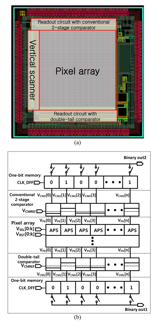
(a) Layout of the proposed CMOS binary image sensor. (b) Block diagram of the CMOS binary image sensor processing system.
The output signals of the vertical scanner, namely, VSEL and VRST, are fed into each row of the pixel array. VPX, which contains information about the incident light, is fed into the columnparallel circuits. The output signals of the pixel array are fed into the comparator, which is either a conventional two-stage comparator or the double-tail comparator. The comparator compares the reference voltage (VCMREF) and VPX and consequently converts an analog signal into a binary signal. The converted binary signal is stored in the 1-bit memory, and the output signal of the horizontal scanner is fed into each column switch of the column array. Thus, the output of the column array produces a binary image signal.
Fig. 3(a) and 3(b) show the schematics of the column readout circuits with a conventional two-stage comparator and double-tail comparator, respectively. Both circuits have the same structure with the exception that conventional two-stage comparator uses VCMBIAS whereas the double-tail comparator uses the clock signal.
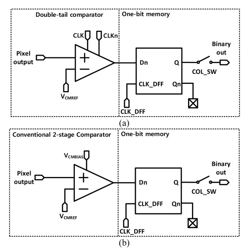
(a) Schematic of the unit column readout circuit using a double-tail comparator. (b) Schematic of the unit column readout circuit using a 2-stage comparator.
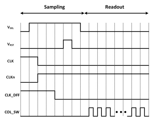
Fig. 4 shows the timing diagram of the CMOS binary image sensor for a row operation. When VSEL is high, a selected row is connected to the column line. When CLK falls and CLKn rises, the double-tail comparator converts the analog signal (a pixel output signal) into a digital signal. When CLK_DFF falls, the 1-bit memory stores the output of the comparator. The COL_SW of the horizontal scanner is fed into each column switch of the column array such that the output of the column array produces a binary image signal.
2.3 Double-tail comparator
Fig. 5(a) shows the schematic of a conventional two-stage comparator, which operates continuously based on the bias voltage of M1. The two input signals (VINP and VINM) are compared continuously. If VINP > VINM, the output is high (1). If VINP < VINM, the output is low (0). As the conventional two-stage comparator continuously compares these two signals, current flows continuously.
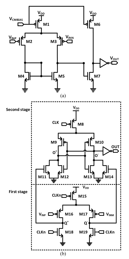
Schematics of (a) the conventional two-stage comparator and (b) the proposed double-tail comparator.
Fig. 5(b) shows the schematic of a double-tail comparator. CLK and CLKn denote the clock signal and inverted clock signal, respectively. Q+ and Q-are the outputs of the first stage, whereas O+ and O-are the outputs of the second stage. If VINP > VINM, the output is high (1). If VINP< VINM, the output is low (0). The double-tail comparator compares the two input signals, causing the current to flow when CLK and CLKn are changed. Therefore, the power consumption of the double-tail comparator is less than that of the conventional two-stage comparator.
Both comparators convert analog signals to binary signals. The conventional two-stage comparator operates continuously; however, the replaced double-tail comparator operates when the clock signal is changed. The signal processing speed of the double-tail comparator is higher than that of the conventional twostage comparator. Consequently, a double-tail comparator is best suited for the CMOS binary image sensor.
3. MEASUREMENT RESULTS
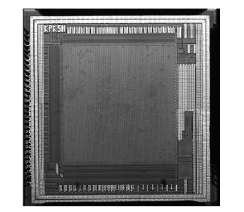
Fig. 6 shows the chip of the fabricated CMOS binary image sensor, which is wire-bonded to a sensor board.
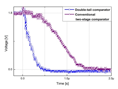
Fig. 7 shows the variation of the measured output voltage with time. The delay time of the conventional two-stage comparator denotes the time difference between the time at which VINP and VINM become equal and the time at which the output of the twostage comparator is 0.9 V. The delay time of the double-tail comparator equals the time difference between the time at which CLK reaches 0.9 V and the time at which the output of the double-tail comparator reaches 0.9 V.
Fig. 7 shows the variation of the fall time of the double-tail comparator, which is shorter than that of the conventional twostage comparator. The fall times of the conventional two-stage comparator and double-tail comparator are 945 ns and 277.5 ns, respectively, and the delay times are 880 ns and 163.7 ns, respectively.
Table 1 presents a comparison of the analyzed comparators. The delay time of the double-tail comparator is shorter (163.7 ns) than that of the conventional two-stage comparator (880 ns), which corresponds to a reduction of 81.47%. Furthermore, the power consumption of the column array decreased from 17.43 mW to 8.32 mW, corresponding to a reduction of 52.27%.
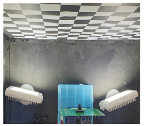
Fig. 8 shows the measurement system setup for image acquisition using the proposed sensor. The power supply provides voltage and current to the motherboard and printed circuit board. The subject is irradiated with light using a light source. The light reflected from the subject enters the image sensor through the lens; the distance between the CMOS binary image sensor and the subject is 32 cm, and the light incident on the subject is 1350 lux.
Fig. 9(a) shows the original subject and imaging region. The image incident on the sensor is converted as shown in Fig. 9(b).
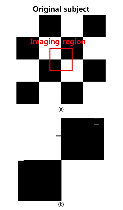
(a) Original subject and imaging region. (b) measured binary image with an array of 16 × 111 pixels for 2000 FPS.
4. CONCLUSIONS
A CMOS binary image sensor with a GBT PMOSFET-type photodetector and double-tail comparator was proposed for a lowpower, high-speed operation. The sensor was designed and fabricated using a standard 0.18 μm CMOS process. Replacing a conventional two-stage comparator with a double-tail comparator decreases the time delay of the comparator and the power consumption of its column array by 81.47% and 52.27%, respectively. Therefore, it is confirmed that the proposed CMOS binary image sensor with a double-tail comparator has advantages such as a high signal processing speed and low power consumption. The proposed sensor can be used in applications such as barcoding, motion detection, fingerprint detection, and text recognition.
Acknowledgments
This research was supported by the Basic Science Research Program through the National Research Foundation of Korea (NRF) funded by the Ministry of Education (2018R1D1A3B0704995214), the Samsung Electronics Company, the BK21 FOUR project funded by the Ministry of Education, Korea (4199990113966), and the Integrated Circuit Design Education Center (IDEC) in Korea.
REFERENCES
- B. S. Carlson, “Comparison of Modern CCD and CMOS Image Sensor Technologies and Systems for Low Resolution Imaging”, Proc. IEEE Sens., Vol. 1, No. 1, pp. 171-176, 2002.
-
E. R. Fossum and S. Member, “CMOS Image Sensors: Electronic Camera-On-A-Chip”, IEEE Trans. Electron Devices, Vol. 44, No. 10, pp. 1689-1698, 1997.
[https://doi.org/10.1109/16.628824]

-
S. Mehta, A. Patel, and J. Mehta, “CCD or CMOS Image sensor for photography”, 2015 Int. Conf. Commun. Signal Process. ICCSP 2015, pp. 291-294, Melmaruvathur, India, 2015.
[https://doi.org/10.1109/ICCSP.2015.7322890]

-
M. Bigas, E. Cabruja, J. Forest, and J. Salvi, “Review of CMOS image sensors”, Microelectron. J., Vol. 37, No. 5, pp. 433-451, 2006.
[https://doi.org/10.1016/j.mejo.2005.07.002]

-
C. Y. Chao, S. Yeh, M. Wu, K. Chou, H. Tu, C. Lee, C. Yin, P. Paillet, and V. Goi, “Random Telegraph Noises from the Source Follower, the Photodiode Dark Current, and the Gate-Induced Sense Node Leakage in CMOS Image Sensors”, Sensors, Vol. 19, No.24, pp. 5447-5465, 2019.
[https://doi.org/10.3390/s19245447]

-
W. Zhang and M. Chan, “A high gain N-Well/Gate tied PMOSFET image sensor fabricated from a standard CMOS process”, IEEE Trans. Electron Devices, Vol. 48, No. 6, pp. 1097-1102, 2001.
[https://doi.org/10.1109/16.925233]

-
H. H. Lee, S. H. Jo, M. Bae, B. S. Choi, J. Kin, H. K. Lyu, and J. K. Shin, “Highly sensitive gate/body-tied metaloxide-semiconductor field-effect transistor-type photodetector with wavelength-selective metal grid structure using standard complementary metal-oxide-semiconductor technology”, Sensors Mater., Vol. 27, No. 1, pp. 135–142, 2015.
[https://doi.org/10.18494/SAM.2015.1079]

-
B. S. Choi, S. H. Jo, M. Bae, J. Kim, P. Choi, and J. K. Shin, “High-Speed CMOS Binary Image Sensor with Gate/ Body-Tied PMOSFET-Type Photodetector”, J. Sens. Sci. Technol., Vol. 23, No. 5, pp. 332-336, 2014.
[https://doi.org/10.5369/JSST.2014.23.5.332]

- J. Lee, B. S. Choi, D. Seong, J. Lee, S. H. Kim, J. Lee, J. K. Lee, and P. Choi, “CMOS Binary Image Sensor with Gate / Body-Tied PMOSFET-Type Photodetector for Low-Power and Low-Noise Operation”, J. Sens. Sci. Technol., Vol. 27, No. 6, pp. 362-367, 2018.
-
H. Kwen, S. Kim, J. Lee, P. Choi, and J. Shin, “Simulation of High-Speed and Low-Power CMOS Binary Image Sensor Based on Gate / Body-Tied PMOSFET-Type Photodetector Using Double-Tail Comparator,” J. Sens. Sci. Technol., Vol. 29, no. 2, pp. 82–88, 2020.
[https://doi.org/10.5369/JSST.2020.29.2.82]

-
D. Schinkel, E. Mensink, E. Klumperink, E. Van Tuijl, and B. Nauta, “A double-tail latch-type voltage sense amplifier with 18ps setup+hold time”, Dig. Tech. Pap. -IEEE Int. Solid-State Circuits Conf., pp. 314-316, San Francisco, CA, USA, 2007.
[https://doi.org/10.1109/ISSCC.2007.373420]

- S. Chaudhari and M. Pawar, “Design of efficient double tail comparator for low power”, 2015 Int. Conf. Commun. Signal Process. ICCSP 2015, pp. 1782-1785, Melmaruvathur, India, 2015.
-
S. Mashhadi, “Analysis and Design of a Low-Voltage Low-Power Double-Tail Comparator”, IEEE Trans. VLSI Syst., Vol. 22, No. 2, pp. 343-352, 2014.
[https://doi.org/10.1109/TVLSI.2013.2241799]

